Reduce CM Noise in Your Power Supply with Impedance Balancing

Simple switching regulator circuits that operate in compact spaces, like on a small PCB, can usually be deployed in noisy environments without superimposing significant noise on the output power level. As long as you lay out the board properly, you’ll probably only need a simple filter circuit to remove EMI on the inputs and outputs. As the regulator becomes larger, both physically and electrically, noise problems can become much more apparent, namely radiated EMI and conducted EMI in the PCB layout.
Common-mode conducted currents are a typical problem in DC-DC converters with multiple grounds, which arises due to capacitive coupling. The standard method is to use filtering on the output, such as with a common-mode choke, to deal with the conducted common-node noise reaching the output node. However, this does nothing to suppress the radiated EMI that exists in the common-mode current loop, leaving you with shielding as the last option. What if you can suppress both types of noise with less need for shielding?
In these types of switching converters, you can use an impedance balancing approach to suppress common-mode noise at the output node from your power supply. This follows a simple idea, where the system ground gets used as a global reference for defining the impedance on the output nodes of your power supply. Let’s look at how this works and what you should investigate with simulations in your design.
What is Impedance Balancing?
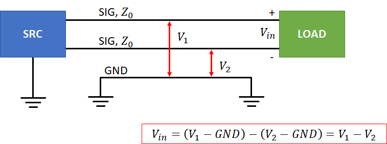
Impedance balancing uses a 3-conductor configuration (2 signal, 1 GND) to gather a differential voltage measurement with an amplifier. This technique is used in XLR audio cables as a means to ensure a differential receiver can fully cancel common-mode noise that might be conducted through the cable. Mark Harris discusses this briefly in a recent blog post, although this was done in the context of sensors rather than audio or power supplies.
The central idea is to set the impedances of the two signal wires to be equal, which will ensure each single-ended side of the cable sees the same input impedance at the receiver and common-mode noise rejection is ensured at the differential receiver.

If you think about it, the arrangement of signal lines and ground in this system is no different than differential pairs on a PCB. In a differential pair, each trace has its single-ended impedance defined with respect to the pair’s reference plane (in this case, a ground plane). The only difference between impedance balancing and differential signaling is that, in an impedance balanced interconnect, we don’t need to have equal and opposite signals for V1 and V2; they could theoretically be any value. The receiver then measures the voltage across each pair with respect to the reference plane.
Impedance Balancing in a Switching Converter
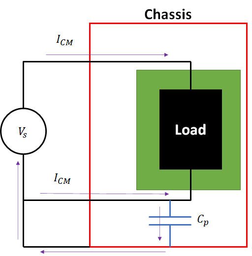
Common-mode noise in a switching converter occurs due to capacitive coupling back to the nearest reference plane, which is typically the chassis GND, or it could be another large conductor that is part of the system GND or enclosure shielding. This can be very problematic in physically large power supply layouts that source high current; the parasitic capacitance Cp (see below) can be very large, giving very low impedance during a high dI/dt switching event in the switching converter circuit.

From here, we can see that the purple arrows trace out a large current loop. Even if we remove the conducted currents at the load with a common-mode choke, there will be strong radiated emission from the common-mode current loops. This can also happen in switching converter topologies that use galvanic isolation with a transformer, such as an LLC resonant converter.
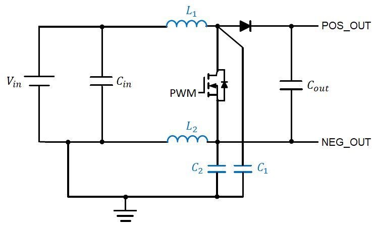
One solution in the following boost converter circuit is to place capacitors around the inductor back to chassis ground, but before the POS_OUT and NEG_OUT terminals. Here, the negative rail is tied back to the system ground at the source V1, which can facilitate a path for common-mode noise between the negative rail and the rest of the system. The addition of capacitors C1/C2 and inductor L2 creates a bridge circuit for the path followed by common-mode noise flowing into the MOSFET:

By intentionally using capacitors to tie the high and low rails back to ground, you will set up two counter-propagating currents in the layout that mimics a bridge circuit. The resulting common-mode noise is eliminated when the following impedance condition holds:

This is discussed in much more detail in the following reference:
Finally, similar strategies have been discussed for differential ADC inputs and motor drivers in the presence of power supply noise:
- Bae, Bumhee, et al. "On-chip design techniques for reducing power supply noise effects on ADC with chip-PCB hierarchical structure." In 2012 IEEE International Symposium on Electromagnetic Compatibility, pp. 549-553. IEEE, 2012.
- Chen, Ruirui, et al. "Common-mode noise reduction with impedance balancing in DC-fed motor drives." In 2018 IEEE Applied Power Electronics Conference and Exposition (APEC), pp. 2515-2520. IEEE, 2018.
Once you create the PCB layout, you should make sure to implement symmetric routing on the high and low sides of the MOSFET. This is important as it will set up counter-propagating current loops that will generate anti-parallel magnetic fields. Any portion of your routing that is not part of common-mode noise cancelation will have differential-mode radiated emission, which is significantly weaker than emission from common-mode currents.
Simulate Impedance Balancing With Parasitics
In the above circuit, it’s important to remember that all of the components have some parasitics and self-resonance, meaning the impedance relationship above will only hold up to a specific frequency. If you use components with higher self-resonant frequencies, you can remove common-mode noise up to much higher frequencies. Make sure to simulate the transfer function of this filter circuit to see the limits of noise suppression in this system.
With the best PCB design tools in Altium Designer®, you can easily design your circuits and simulate an impedance balancing scheme for removing common-mode noise. You can also instantly capture your schematics in a blank PCB layout with a complete set of design tools in a single application.
When you’ve finished your design, and you want to release files to your manufacturer, the Altium 365™ platform makes it easy to collaborate and share your projects. We have only scratched the surface of what is possible to do with Altium Designer on Altium 365. You can check the product page for a more in-depth feature description or one of the On-Demand Webinars.
