What is Multi-board Design?
Many complex electronics systems are built as multi-board arrays of PCBs. There are some advantages to this type of system design, such as the modularity you’ll see in platforms like Arduino and Raspberry Pi. Other common types of circuit boards like flex and rigid-flex systems are multi-board systems and require a common PCB layout and routing strategy. If you want to develop your own multi-board system, there are some basic steps you can take to ensure your design will have the connectivity you need.
Creating a multi-board system is a lot easier when you use the best PCB design software for your board. The PCB tool sets you need in your design software include standard electrical utilities, as well as MCAD integration to ensure your boards mate properly. In this short guide, we’ll cover some of the basic aspects of defining connectivity in your design while also ensuring signal integrity in the design. Whether working with standard rigid multilayer PCB design and layout or more involved flex/rigid-flex circuit boards, there are some basic design tool sets you’ll need to ensure your design works as intended.
- Planning Your Multi-board PCB System Design
- Native 3D PCB Design for Multi-Board Assemblies
- Routing in Multi-Board Systems
Multi-board design starts with a mechanical outline of each board in your system and a plan for how they will connect to each other. Your connection style could involve simple standardized connectors, such as mezzanine connectors or pin headers, or integrated edge connectors. Once these points are determined, a placement and routing strategy needs to be developed so that components can properly connect to each other throughout the design without creating EMI/EMC, SI/PI, and mechanical vibration problems. Read the sections below to see how you can get started with high speed design and the important role of your PCB design software.
Planning Your Multi-board PCB System Design
Designing a multi-board PCB arrangement is a system-level design project and involves defining connections between all the boards in your system. A good process to start floorplanning your multi-board PCB system is as follows:
- Determine a board arrangement: How will the boards be oriented with respect to each other? Does the system have a moving element that needs to interact with the board somehow? Mechanical modeling needs to begin at this stage and will determine how the design
- Choose connectors: Will your boards interconnect with off-the-shelf board-to-board connectors, edge connectors, flex ribbons, or cables? Connectors need to be chosen to support your required board arrangement while still fitting into your enclosure.
- Decide board functions: Ideally, each circuit board in a multi-board system will perform specific functions and should hold only the components required to support that function. This might force you to rethink your board arrangement and connector options, so be thoughtful of this when deciding which functions to place on which boards.
- Map signals across connectors: Each connector should support specific signals or groups of signals, as well as ensure signal integrity in the design. Pinouts can be determined in this stage and can be defined on schematic symbols for connectors.
- Start creating schematics: To stay organized, it’s best to segment schematics so that they reflect the arrangement of your boards in your multi-board system layout. Each set of schematics should only contain components from a single board, components from different boards should not be placed in the same schematic sheets.
After creating schematics for each board in the system, it’s time to start creating the physical PCB layout for each circuit board. Follow the standard process for PCB design to import your components into your design and place them around each board. At this point, connectors can be placed in the intended positions on the PCB, and edge connectors can be defined on specific components.
- Learn more about the creating schematics for your PCB
- Learn more about creating a PCB layout from a schematic
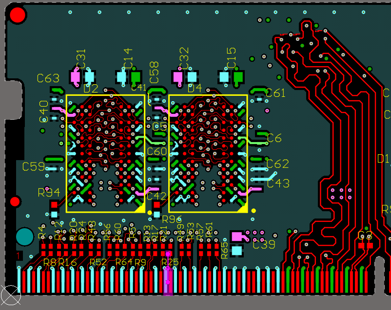
Before you start routing components, it’s important to start thinking about your mechanical requirements and whether you can still fit the design into its intended enclosure after the layout is finished. Doing this requires working with a model of the enclosure and each board in the system to ensure there are no interferences and boards will fit together as intended.
Native 3D PCB Design for Multi-Board Assemblies
Some measurements and modeling are very difficult in 2D, which creates a risk of interference between your circuit board, the components, and the enclosure. In multi-board PCB design, a PCB assembly involves multiple boards, and there could be unwanted interference between boards in the design, or between components, cables, and other elements in the system. The best way to prevent this is to incorporate mechanical backchecking into the design process to ensure there are no interferences.
During backchecking, clearances are automatically checked in 3D using MCAD tools that examine a 3D model of your board, your enclosure, and your components. The standard 3D modeling file format in MCAD software and PCB design features is a STEP model. By combining STEP models for each component in your design, your design software can create a realistic model of the board.
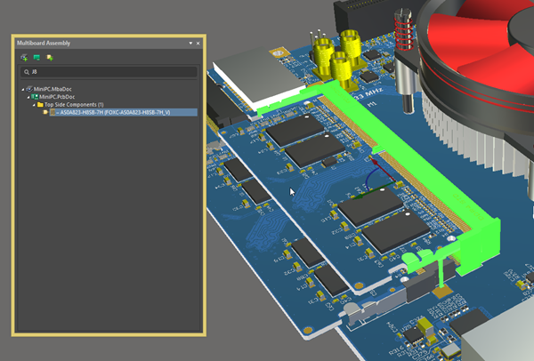
If you’re working with a mechanical designer to build your multi-board design, they should provide a model of the PCB enclosure for the design. This can then be imported into your PCB design software to perform interference checking inside your ECAD tools. The other option is to export a STEP model or IDF file for the board, which can then be imported into an MCAD application for backchecking. The standard workflow in enterprise-level teams is for the MCAD user to perform backchecking so that component placement can be verified.
After the initial placement on all boards is completed and checked for interferences, the design is ready for routing. Multi-board systems require a few important routing considerations with high-speed signals and lower-speed digital protocols to ensure signal integrity.
Routing in Multi-Board Systems
In each board, routing should be performed after setting up initial design rules, calculating any required impedance profile, and setting the design into the appropriate routing mode. While high speed interfaces are not present in every circuit board, they can be routed between boards in a multi-board system through an edge connector, cable, flex ribbon, or board-to-board connector. Slower single-ended signals (e.g., from GPIOs) or bus protocols can also be routed over cables and between boards. However, care must be taken to ensure uniform grounding and to prevent signal integrity problems that can arise.
Defining Ground in Multiboard Systems
Just like in other PCBs, ground in a multi-board layout needs to be clearly defined to ensure routability for your signals. When routing signal paths between boards, use the following process to ensure a consistent ground potential is enforced throughout the system:
- Use ground planes in each board to provide a clear characteristic impedance, provide shielding to suppress EMI/crosstalk, and help provide strong decoupling in the PDN.
- When routing between the two boards, include a ground connection across the connectors so that the ground regions in each circuit board are connected. This will provide shielding across the connector or cable.
- For ribbon cables or twisted pair cables, consider using interleaved ground between signals to provide a clear reference and stronger shielding in the routing path.
This simple use of ground when routing across a connection between circuit board designs in a multi-board system is an important part of signal integrity. This helps define consistent impedance, return paths, and crosstalk suppression in multi-board PCB design and routing. If you’ve followed these steps, you’re much more likely to maintain signal integrity for single-ended signals as you route between boards and over cables.
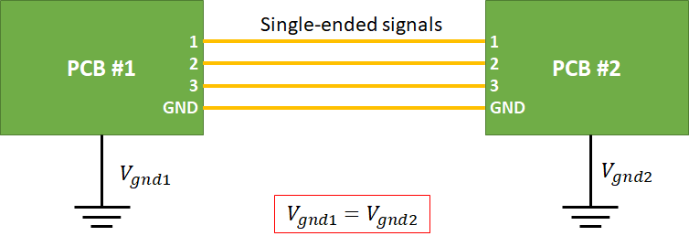
Unfortunately, there are some multi-board systems that have a topology where this type of ground connection can’t be provided. This is often the case when the system is physically spread out over multiple cabinets, rather than having all the boards connected in the same enclosure. However, there are times where boards are daisy chained in the same cabinet and supply high power, in which case the design may create a safety and reliability problem that is only solved with differential pair routing.
Why Differential Protocols Are Used in Multi-board Design
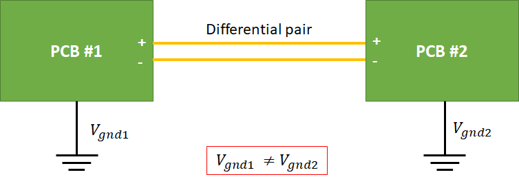
When routing over long cables, such as in industrial systems, a better approach is to use differential protocols for routing. Larger systems with grounded connections between boards, particularly in DC systems where the ground can carry high current, can be a safety hazard and can cause the cable to become damaged as the cable dissipates high heat in the ground connections.
In the case where shielding is being used on larger systems connected with cables, particularly in linear arrangements of boards in series, the ground planes in each circuit board should be isolated and not connected to each other. Instead, the chassis and an earth connection should be used for shielding, not the PCB ground plane. Then, to route signals between boards, differential pairs should be used as they can accommodate a ground offset between boards in a multi-board system.
The primary reason that differential protocols are used in multi-board systems is they eliminate the need for a clear ground reference when routing between two circuit boards in the system. Once the differential pair comes back onto a board and the difference signal is read, the data can be recovered without worrying about the ground offset that occurs during routing. Common differential protocols for routing between PCBs in a multi-board system include CAN bus, Ethernet, and RS485.
When you need to build advanced high speed digital systems while ensuring you maintain signal integrity and power integrity, use the best set of high speed design and layout tools built on a rules-driven design engine. Whether you need to layout a dense single-board computer or a complex mixed-signal PCB, the best PCB layout tools will help you stay flexible as you create your multi-board design and the PCB layout for each of your circuit boards.
Multi-board system design engineers, PCB layout engineers, and SI/PI engineers trust the advanced design tools in Altium Designer® for their design and layout needs. When you’ve finished a design and are ready to release it to manufacturing, the Altium 365™ platform makes it easy to collaborate and share your projects. Altium Designer also integrates with popular MCAD and simulation applications, giving you the ability to better understand power and signal behavior in multi-board systems.
We have only scratched the surface of what’s possible with Altium Designer on Altium 365. Start your free trial of Altium Designer + Altium 365 today.
