LLC Resonant Converter Design and PCB Layout

DC-DC converters can be difficult to design and can even be dangerous, particularly when we consider switching converters with high current output. Among the various types of switching converters and their topologies, LLC resonant converter designs are not often discussed until you look at application notes from power electronics companies. These converters are key portions of high power systems like LED banks, appliances, desktop and server power supplies, and many other power conversion systems.
Once you look at control algorithms and methods for implementing a feedback loop, an LLC resonant converter design starts to show its value. You could implement the same type of control algorithm you might use for a buck-boost converter to accommodate a power supply with droop or excessive ripple, but you can get to higher output powers with this type of isolated switching converter. When you’re ready to create your PCB layout for these systems, there are some points you should remember for safety, heat management, and noise suppression.
LLC Resonant Converter Design
An LLC resonant converter is a switching converter that controls the output voltage by selecting the appropriate frequency for a switching signal. Contrast this with a standard switching converter (e.g., buck or boost topology), where the output is controlled through the duty cycle of a switching signal. These systems enjoy many high power applications, including in systems with AC mains input.
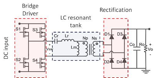
The block diagram below shows the various portions of an LLC resonant converter. The input stage of the converter generally consists of a rectifier, power conditioning stage (PFC circuit), and smoothing capacitor bank. An EMI filter may be placed here if we’re dealing with AC mains. Note that the PFC stage is not strictly required for an LLC resonant converter design, but it will keep power conversion efficiency high, just like in any other switching regulator.

Full Bridge vs. Half Bridge Switching
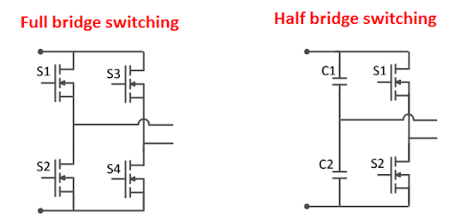
The switching element in an LLC resonant converter design is provided in two possible configurations. In a full-bridge switching circuit, we have 4 MOSFETs, while a half-bridge switching circuit has 2 MOSFETs. These elements switch on and off in the same way diodes in a bridge rectifier switch between forward and reverse bias when supplied with AC power. Here, the full-bridge will generally take up more space and generate more noise. I prefer a half-bridge switching circuit as the capacitor required for frequency control can be placed directly in the half-bridge circuit (C1 and C2).

Output Rectification
Rectification on the output side can be applied in a number of ways. The goal here is to control the direction of current so that the output is always DC. The capacitors in the output side will smooth out any ripple when the bridge section switches. In simpler LLC converters, output rectification is provided by diodes, while a higher current LLC resonant converter design may use MOSFETs to provide rectification on the output side.
Controlling the Output
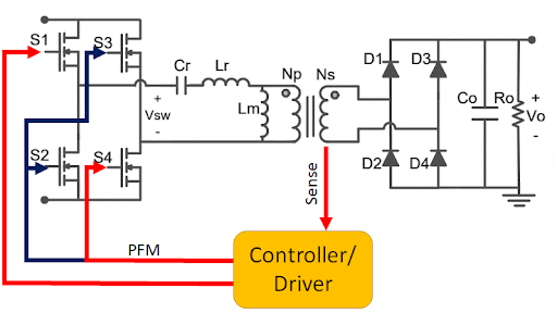
The output is set by selecting the appropriate turns ratio on the transformer, just as you would with an AC circuit. However, the magnitude of the voltage seen at the primary side of the transformer is controlled by adjusting the frequency of a driving signal sent to the switching circuit. This driving signal is a pulse-frequency modulation (PFM) signal with ~50% duty cycle.
The LC resonant tank circuit will have some gain as the only resistance in the circuit is the MOSFETs’ on-state resistance and the winding resistance of the transformer/inductor coils. Typical gain values are 1 to 1.5. As the output power drops, the driver needs to adjust the PFM signal frequency and bring the system closer to resonance. In this way, the output power can be increased by exploiting just enough gain on the primary side of the transformer.

This type of control method is simple enough to implement with a feedback loop, current or voltage sensing circuit, and an MCU, as shown in Figure 3. There are also specific components that can provide this sensing functionality and provide the pulse signal needed to drive the bridge circuit. Once you finish designing your circuitry and you’ve selected all your required components, you’ll need to think about how to bring it all into your PCB layout.
Component Placement in Your PCB Layout
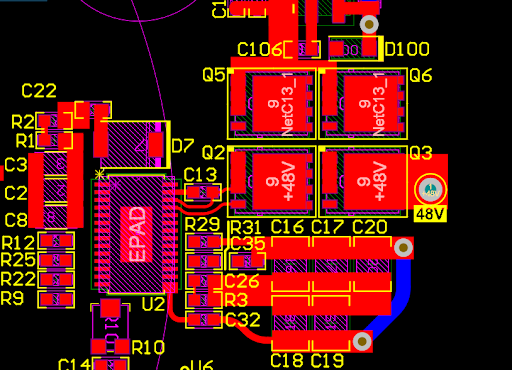
As LLC resonant converter designs are normally used in moderately high voltage systems, there are a few basic design tips to follow:
- Output transformer: Follow best practices for isolated DC power supplies when placing the final transformer. The transformer will isolate the high voltage side from the output, but be careful with this; an operator could still be exposed to high voltage from the feedback loop.
- MOSFET rectifier: For high current output systems, you may end up using MOSFETs on the output side to provide rectification of high currents. A group of MOSFETs might even be used in parallel on the output side in order to provide large current without risking breakdown.
- Clearances: If you’re operating at high voltage, take advantage of clearance design rules in your PCB design tools. You’ll want to ensure your board does not violate safety standards on clearances between conductors with high potential difference between them.
As is the case in most high power systems, the layout will most likely need heatsinks, fans, or both, either mounted to particular components. For something like an LED board, which might run at 500 W or more, your best bet is to use a metal-core PCB as the metal core will provide natural heat dissipation. Thermal vias on critical pads can also help here by dumping heat into a plane layer.
When you’re ready to create your next LLC resonant converter design, use the schematic editor and PCB layout tools in Altium Designer®. Once you’ve created your schematics and PCB layout, you can share your design data on the Altium 365® platform, giving you an easy way to work with your design team and manage your design data.
We have only scratched the surface of what is possible to do with Altium Designer on Altium 365. You can check the product page for a more in-depth feature description or one of the On-Demand Webinars.

