SMPS Circuit Design: Which Switching Frequency to Use?
Power supply on a network switch
Power electronics and switched-mode power supply (SMPS) designers should know that working with higher switching frequencies can lead to higher switching losses in your system. However, the push to miniaturize power supplies, and the components that go into them, compels designers to work with higher switching frequencies in their SMPS circuit designs. This then creates problems where switching losses and noise can become severe in your system.
Like most engineering decisions, choosing the right switching frequency represents a set of trade-offs that involve reducing component size, reducing losses, and removing noise; it can be difficult or impossible to achieve all three of these simultaneously. However, with some smart PCB layout decisions, you can balance the need for higher frequencies and edge rates in your SMPS circuit with the need to keep noise to a minimum.
Optimizing Frequency, Loss, and Noise in an SMPS Circuit
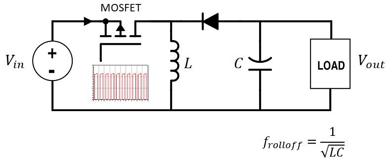
In order for an SMPS to operate with smaller components, the switching PWM signal must run at a higher frequency. The output inductor, capacitor and diode are designed to pass DC power through the output while filtering the switching noise, any residual ripple from the input voltage (e.g., from a rectifier circuit), and any spurious harmonics that may be present at the input. In other words, the output acts like a low pass filter (really, this is an RLC bandpass filter) within a certain bandwidth. We can define a rolloff frequency for this filter (not to be confused with the knee frequency of a switching digital signal).
In order to prevent PWM switching noise from propagating through the output, the PWM switching frequency must be larger than the rolloff frequency of the circuit. Whether you are working with a buck or boost topology in your SMPS circuit, the rolloff frequency of the output will be inversely proportional to the output capacitance and inductance. In other words, you can use smaller components in your SMPS circuit if you use a sufficiently high PWM switching frequency.

Buck-boost SMPS circuit diagram
It is generally assumed that the switching frequency of the PWM signal in your SMPS circuit will be the primary determinant of losses, which are then converted to heat. This issue with using a higher frequency is correct, but the frequency is not the only parameter that determines losses in the MOSFET. In reality, with power MOSFETs used in SMPS circuits, the edge rate is an important determinant of the heating losses in the SMPS circuit.
No circuit element is ideal, but we tend to treat them as such when it is not appropriate. The same applies to the MOSFET shown above. When the PWM signal drops to 0 V, the MOSFET may not turn off completely and can continue conducting when the edge rate is too slow. If you increase the PWM signal edge rate, the MOSFET can be fully cycled and it will conduct less in the OFF state. This actually reduces power loss, even when the switching frequency is set to a higher value.
The combination of a higher PWM frequency and faster PWM edge rate allows smaller components to be used in the SMPS circuit. Because power losses (i.e., heat dissipation) are lower, a smaller heat sink can be used. However, the higher frequency PWM signal radiates strongly, and the faster edge rate leads to a transient response in the circuit. This behavior is entirely related to parasitic capacitance and inductance at the MOSFET package and board layout levels. You’ll need to ensure your SMPS circuit is laid out in such a way that parasitic inductance is minimized.
Reduce SMPS Noise Spikes With Smart Layout Choices
The parasitic inductance in your SMPS circuit (which includes the downstream PDN) will determine the size of the voltage spike in the SMPS circuit. The parasitic capacitance also contributes to voltage/current spikes in the SMPS circuit, but this does not dominate until you are working at kV levels. This particular voltage spike, due to parasitic inductance, occupies circuit loops in your SMPS layout, which can stress components to the point of failure.
If you use a faster edge rate, you will induce a larger transient current in your SMPS circuit. Even a relatively short trace (a few cm) on standard-thickness FR4 will have ~10 nH of parasitic inductance. A fast rising edge in the PWM signal with an ON current of a few amps can induce a spike of several volts. Over time, this stresses components and leads to failure of the SMPS.
With a higher switching frequency and faster PWM edge rates, you can use smaller components than this inductor and these capacitors.
Overcoming this challenge can be difficult as it requires extracting the parasitics in the SMPS circuit. The typical strategy when designing one of these circuits is to run simulations from your schematic to verify functionality, followed by testing once you spin a prototype. Hopefully, with the guidelines outlined here, you can reduce the number of prototyping spins required to get to a working device.
The design tools in Altium Designer® are ideal for designing your SMPS circuit and creating a strong layout that you can take to fabrication and assembly. With the pre-layout and post-layout simulation tools, you can examine your design before moving to manufacturing. Now you can download a free trial of Altium Designer and learn more about the industry’s best layout, simulation, and production planning tools. Talk to an Altium expert today to learn more.
