PCB Routing Guidelines for Altium Designer
Routing traces and vias on a PCB design is often thought of as a simple task. After setting up the footprint library and then perfecting the placement of the components on the board, it would seem a relatively easy matter to simply “hook ‘em up.” While that may have been true back in the days of routing low-speed TTL DIP components on simple boards, today’s design requirements are much more complex.
Whether you’re working through a high-speed PCB layout or a lower speed digital board with multiple bus protocols, you’ll need the best PCB routing tools you can find. Routing copper traces is much easier when you can automate compliance with your PCB design rules using the best PCB layout tools. Whether you’re an Altium Designer user, or you use a different PCB design application, follow these PCB routing guidelines to ensure your board maintains signal integrity and will comply with all your PCB routing rules.
ALTIUM DESIGNER
The industry’s best PCB design software with a complete set of layout, routing, and analysis tools for professional designers.
The electronics used in PCBs have been getting faster, smaller, and denser. Newer designs include multiple low-speed and high-speed routing protocols and components, and designers need to be aware of PCB routing guidelines in each domain. Simpler PCB designs carry some basic routing rules that all designers should know, but advanced high-speed signaling standards require careful consideration of impedance, propagation delay, and much more.
There are specific size and topology rules for power, differential pair, high-speed, RF, and rigid-flex printed circuit board design routing technologies to name a few of the challenges that engineers face today. The design rules you define in your PCB routing and layout software will help ensure you comply with important signaling and routing requirements. Make sure to follow these routing guidelines in your PCB routing tools so your design operates as intended.
PCB Routing Guidelines for Advanced Electronics
There are many rules and techniques associated with PCB trace routing. Some of the important rules designers need to follow relate to trace geometry, total loss, routing topology, single-ended vs. differential impedance, and allow skew between nets. Your PCB routing tools will help ensure your layout maintains signal integrity, complies with basic routing requirements in your signaling standards, and is manufacturable.
Some of the important design routing requirements you’ll find in low-speed and high-speed signaling standards include:
- Topology: examples include bus routing and point-to-point routing
- Total loss: the maximum length of a given route will depend on the total allowed loss and the characteristics of the PCB substrate material
- Allowed skew: differential pairs, protocols with source-synchronous clocks (SPI or I2C), and parallel buses all have maximum skew specifications
- Impedance: high-speed signals with fast edge rates will have impedance requirements to ensure power transfer into receiver components
- Crosstalk limits: newer high-speed PCB signaling standards set limits on allowed crosstalk between two channels
- Allowed overshoot/undershoot: there are several effects that can cause overshoot or undershoot during a signal transition
Look at your signaling standards to find the important routing requirements you should set in your PCB design rules. Once these are defined in your design, you should still follow some basic routing practices to ensure signal integrity and low EMI.
Ensure Accurate Routing With Rules-Driven Layout Tools
The power of PCB design software like Altium Designer is in its rules-driven PCB design tools. It’s easy to maintain compliance with the above list of requirements when routing low-speed and high-speed signals when you use Altium Designer. The rules-driven design engine checks your PCB layout against your design rules as it’s created, ensuring you only route the highest quality design and follow basic requirements in your signaling standards.
- Successful PCB routing starts with creating the right stackup to support your required trace density, impedance goals, and EMI limits.
Learn more about designing a PCB stackup to support your routing strategy.
- Once you’ve designed your stackup, you can determine required impedance for your high-speed signals.
Learn more about designing your interconnects with required impedance.
- The fiber weave structure in your PCB substrate will influence skew in your design and will determine how your fabricator builds your PCB stackup.
Learn more about fiber weave effects and skew in high-speed routing.

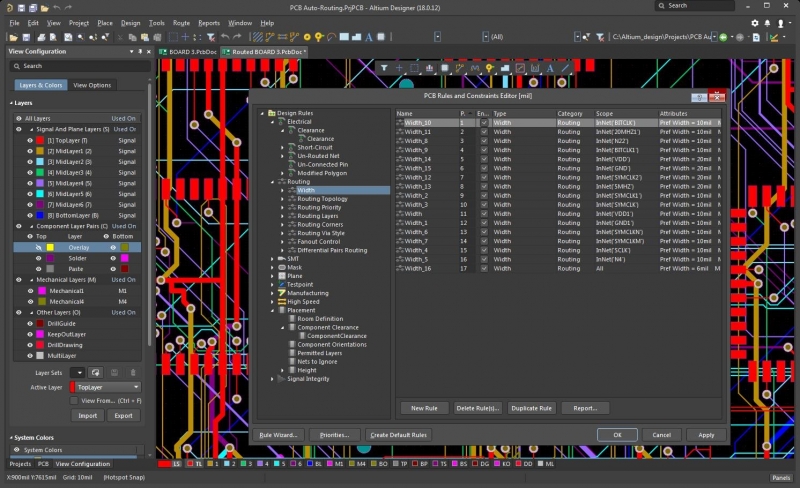
Once you’ve determined your routing requirements, set them up as design rules to ensure accurate PCB routing in Altium Designer.
Maintain Signal Integrity During PCB Routing
In addition to the requirements in your signaling standards, there are some basic routing guidelines that any PCB designer should follow. These guidelines are intended to help prevent signal distortion, suppress EMI, and ensure signal integrity as you route your PCB. With the right routing tools, it’s easy to follow these basic guidelines for successful PCB routing:
- Keep high-speed signals separated enough to prevent crosstalk
- Don’t put ground pour too close to impedance controlled lines
- Don’t route signals over a region without a ground plane
- Don’t make excessive layer transitions through vias as each via causes losses
- Be sure to backdrill vias on very high-speed signal nets to prevent return losses
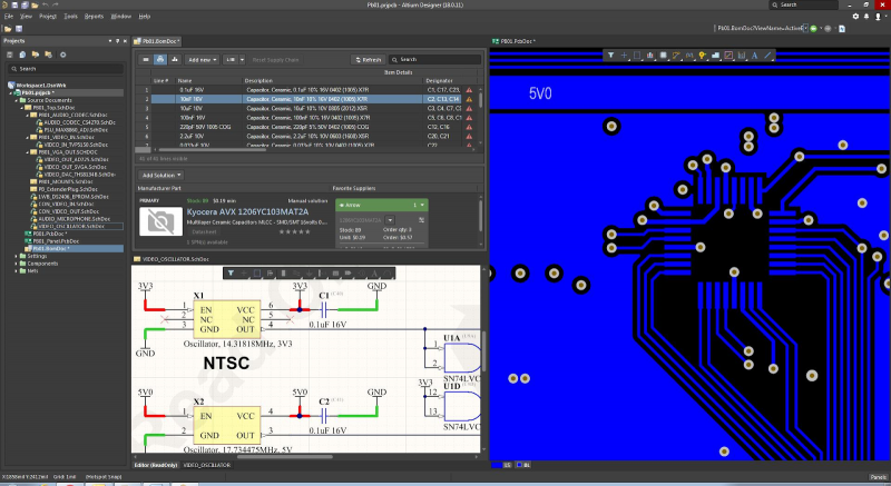
It’s easy to implement these guidelines when you have access to the best PCB routing features alongside your schematic design, schematic capture, circuit board layout, and simulation tools. With adaptive and interactive routing features, it’s easy to take control of your routing and create high-quality PCB layouts that ensure signal integrity.
Powerful and Intuitive Design Tools for the Best Quality PCBs
Whether you need to build high-speed or high-frequency circuit board designs, Altium Designer has the complete set of PCB routing and board layout features you need. Routing with large busses and other time-consuming routing tasks are easy with intelligent interactive routing, high-speed routing, and auto routing features. Stay productive and route successfully with the best set of design tools in a single interface.
- Make sure your PCB routing constraints are programmed into your design rules so that you don’t fall victim to common radiated EMI sources.
Learn more about EMI sources in high-speed and high-frequency PCBs.
- Altium Designer’s layer stack manager lets you set a specific impedance profile for important nets to ensure they always have the right width.
Learn more about impedance profiles for accurate routing in Altium Designer’s stackup tools.
- Complex components like BGAs are easy to fanout and route with the interactive layout and routing features in Altium Designer.

Altium Designer’s interactive routing features provide intelligent semi-automated PCB routing that obeys your design rules and basic routing requirements.
A Complete PCB Layout Toolset for Advanced Electronics
Altium Designer gives you access to much more than advanced PCB routing features. The complete set of PCB design tools in Altium Designer are built to work together in a single application. Altium Designer’s rules-driven design engine makes every PCB design utility you need accessible in a single application, and it helps ensure every aspect of your layout complies with basic design and manufacturability standards.
Altium Designer’s interactive routing features are designed to ensure you have multiple routing options to help you stay productive. When it comes to high-speed design, Altium Designer is equipped with xSignals, an integrated layout simulation engine that analyzes your design to ensure signal integrity as you work. With trace lengths, matched lengths, and trace tuning functionality in your high-speed routing topologies, you will have optimum control over critical signals and nets.
Finish Your PCB Layout and Take it to Manufacturing
Altium Designer helps guide you through the entire PCB design process to ensure your board is manufacturable. When you need to generate your fabrication and assembly files, Altium Designer automates the process and provides the documentation needed to ensure accurate production and testing. From a complete set of schematic and circuit design tools, to powerful PCB routing and manufacturing features, Altium Designer has everything you need to create the most advanced technology in a single program.
- When you need to build the best designs and create advanced electronics, use the only design application with the best routing and layout features.
Learn more about the complete suite of PCB design tools in Altium Designer.
- Altium Designer’s routing engine gives you full control over your trace routing and layout in an intuitive interface.
See Altium Designer’s advanced PCB routing engine in action.
- The Altium 365 platform makes it simple to share project data and collaborate with other designers via a managed cloud platform.
Learn more about sharing your PCB project data with Altium 365.

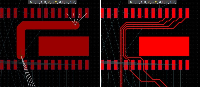
Altium Designer’s Active Route allows you to direct the path of the auto routing
The full suite of PCB routing and layout tools in Altium Designer gives you everything needed to create the most advanced designs you can imagine. When you need to ensure accurate routing and PCB layout in a single application, use the industry’s best set of PCB design tools in Altium Designer.
Altium Designer on Altium 365 delivers an unprecedented amount of integration to the electronics industry until now relegated to the world of software development, allowing designers to work from home and reach unprecedented levels of efficiency.
We have only scratched the surface of what is possible to do with Altium Designer on Altium 365. You can check the product page for a more in-depth feature description or one of the On-Demand Webinars.
