How To Design the Perfect PCB Stack Up With Altium Designer
In the last 20+ years, electronics have become increasingly more complex. Board density is always being pushed to the limits, EMC/EMI regulations evolved and got stricter, and edge rates have become smaller. Therefore, the PCB Layout engineer needs a good understanding of EMC, PDN, EMI, and SI in order to route a modern PCB with confidence. In this article we’ll talk about some of the considerations we should have in order to create a PCB stackup correctly as this relates to the other areas of board design mentioned above.
What Are We Going to Learn?
In this article, we will learn how to plan a PCB stackup and then how to implement it in Altium Designer. We will consider some design optimization to minimize the SI issues in high speed digital designs.
We will learn
- Understand datasheets for PCB laminate materials
- How to estimate the number of required signal layers
- Some suggestions and a brief guide for designing a PCB stackup in Altium Designer
Understanding a PCB Laminate Material Datasheet
The first step a PCB layout engineer should do is to select the appropriate PCB laminate materials (resin, copper foil, and glass weave style) for his/her application. The choice of core and prepreg laminates depends on the type of application. For example:
-
High speed digital boards for typical applications like servers, routers, high speed data channels (e.g., PCIe, 10 Gbe, etc.) may require a laminate like FR408HR, I-speed, etc.
-
High thermal reliability applications like automotive, aerospace, and military may require a laminate like P95/P25 (with high Tg/Td).
-
RF & microwave requires laminates like IS680 TerraGreen (RF/MW) or Rogers.
-
Halogen-free laminates are needed in applications like transportation, mobile products, and wireless devices. TerraGreen is also a good laminate for these systems.
-
HDI (high density interconnect) is used for layer count reduction, military, and aerospace products. Requires a laminate like I-Speed, FR408HR, etc.
-
Polyimide is used for flex or rigid-flex boards, with typical in military, aerospace, and mobile. This requires a laminate like P25N, P95/P25, etc.
In order to select the right material, we need to understand some specs in the PCB datasheet.
Coefficient of Thermal Expansion (CTE)
The (CTE) is usually expressed in ppm/°C. Be careful with this as this is normally quoted as two different values; one is perpendicular to the laminate surface, and the other is along the laminate surface. Usually, it is higher along the z axis than on the x and y axes. This parameter is critical on the z axis. When it is too high during assembly, we may have micro-cracks on vias because the laminate and copper have different CTE values.
Instead, x and y CTE values should be chosen carefully when designing electronics with many thermal cycles. For example, in the aerospace industry, x and y CTE values are very important since LEO satellites have orbital periods of 90-120 minutes, during which time the satellites are exposed to repeated thermal cycles. This frequent cycling between extreme temperatures may cause cracks on the sides of the board.
Glass Transition Temperature (Tg)
The Tg is the temperature at which the prepreg resin transits from rigid to reasonably elastic material. When this temperature is exceeded, the laminate's CTE value becomes very large and more stress can be put on vias and other conductors on the board.
Decomposition Temperature (Td)
As the name suggests, this is the temperature where the prepreg material decomposes and starts to lose its properties.
Dielectric Constant (Dk)
This parameter is an average dielectric constant for the core and prepreg materials. I’m using the word average because if we are looking at the structure of a prepreg weave of glass it will look something like this:
Figure 1: Prepreg fiber weave example
The resin will fill the gaps in the glass structure, creating a dielectric Dk1 zone and one with Dk2. At very high frequencies, this causes some SI, PI, and EMI problems (fiber weave effects). The key point is that, when designing HSD circuits, you need to select a prepreg that is as homogeneous as possible, like I-Speed, FR408HR, Tachyon 100G.
Loss Tangent (Tan(δ)) Or Dissipation Factor (Df)
An electromagnetic waveform traveling through a dielectric material is partially absorbed by the material. This absorption is quantified as a dissipation factor, or Df in a PCB laminate datasheet. This translates into an attenuation per inch using Eq. (1):

where f = frequency in GHz, and ϵR is the dielectric constant of the laminate. Consider this example: Isola FR408HR has ϵR = 3.7 and tan(δ)= 0.011; the attenuation at 10 GHz is -0.94 (dB/in). So, using FR408HR we have lost already -3 dB after just 3 inches.
How Estimate the Number of Signal Layers
In order to design the PCB stackup, we need to guess the number of layers we need. There are two interesting ways to do this.
-
The first way [1] assumes the components with the highest number of pins, e.g., a BGA component, dictates the worst-case scenario. Using this method, you estimate the number of signal layers in the PCB stackup by taking the number of I/O rows (or columns), divide the number by 2, and then round up the result to the nearest even number. E.g. if a BGA has 11 rows/columns of I/Os, then a good guess for the minimum number of I/O layers is 6.
-
The second way is to use Rent’s rule.[2] Rent was an IBM engineer who popularized the way he estimated the average trace pitch. According to the rule, if you have M routing layers and N interconnections [2], the average pitch, in inches, is equal to:

where X and Y are the board’s X and Y dimension in inches. Therefore, you can estimate the number of routing layers by estimating M, and then seeing if the resulting pitch is compatible with the PCB technology.
Reference Plane Considerations
After estimating the number of routing layers, we must decide the number of planes. Some points to remember are:
-
A plane layer provides a return path for high speed signals (always route a critical trace within 2 planes).
-
All planes have structural resonances. Every plane works as an antenna and will resonate at [3]

where n and m are the modes, and W and L are the dimension in mm. For example, if a plane has the dimension of 100mm x 50mm, then the first mode should resonate around 1.34 GHz. Why do we need this information? Because during the EMC testing (Radiated Emission), if we find a peak around 1.34 GHz, which is not a multiple (or intermodulation) of any clock frequencies, then you know that your plane is probably resonating. There are many design techniques to increase the resonance frequency or suppress edge emission, but some of these are beyond the scope of this article.
-
Cavity resonance between planes. To prevent a cavity resonance between 2 that are held at the same potential (e.g. 0V), you can place any vias running in the planes no closer than λ/(10√(εR)) [3].
-
Reduce the Q value for any resonances in the VDD-GND plane. Every VDD-GND plane serves an important rule. It distributes capacitance while it resonates. If it has a high capacitance, it will most likely fail the Radiated Emission. One way to avoid this is to put the 2 planes as close together as possible (increasing the C and reducing the Q).
PCB Stackup Design in Altium Designer
It is now time to design the PCB stackup. From what we wrote above, we already have the following:
-
Number of signal layers
-
Minimum number of planes
-
Critical signal layers (clock, DDR, USB)
-
PCB laminate material
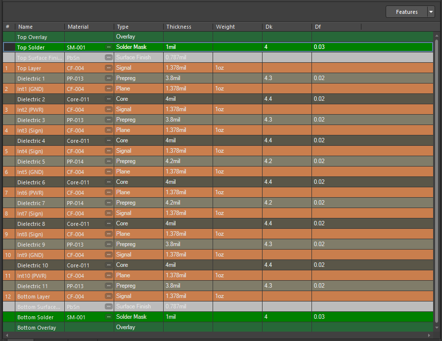
From points 1 and 2, we have a good idea of the number of layers your application needs. Let us say we have about 6 signal layers and 6 plane layers. You can load a preset stackup in Altium Designer using the Layer Stack Manager. Select Tool -> Presets -> 12 Layers to create a default PCB stackup. You can then define each layer as a plane or signal layer. You can also define the dielectric properties (Dk and Df values), as well as the copper weight in each layer. We now need to modify the default stackup with parameters for our particular PCB laminate material.
Layer Arrangement
The default stackup is fine for lower speed boards with low routing density, but it's not the best choice for high-speed PCBs. The image below shows a 12 layer stackup with a typical signal-plane-signal-plane alternating layer arrangement; this arrangement is a good place to start for a high-speed PCB. Note that the layer names in the left column are the default names for the preset stackup; you can change these to whatever you like in order to help your layout and routing process.

If we are not happy with the default materials, you can change them and insert the correct material, thickness, Dk, and Df. You can also load a standard PCB laminate from the Stackup Material Library. This is probably one of the most important pitfalls that happens in PCB stackup design: choosing a stackup that does not match standard materials or the material set available at your manufacturer. Be sure to check that your stackup material is available and that your laminate thickness matches your vendor's specifications. This becomes quite important in the next task as the impedance of your traces will depend on the laminate thickness.
Impedance Control
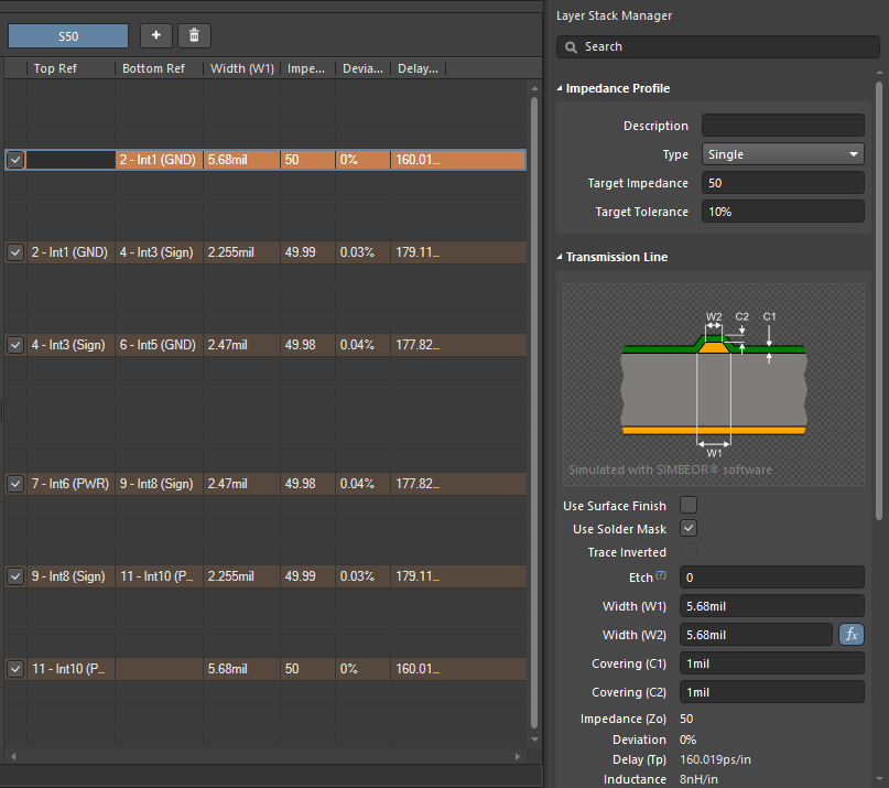
Once we are happy with the material, we must decide which layers to use for signals, critical signals, and planes. We can start planning the critical signals first (for example clock traces, DDR nets, etc.). As you start planning which layers will support different nets, you can determine the characteristic impedance and differential impedance for traces on different layers by creating an impedance profile. Simply click on the Impedance tab (at the bottom) and then click on Add Impedance Profile. By default, the profiler tool will calculate the trace width required for a characteristic impedance of 50 Ohms:

For example, according to the above impedance profile, the width of a 50 Ohm trace is around 5.68 mils on the top and bottom layers, while only 2.255 or 2.47 mils is needed in the inner layers. We can use the same tool to determine the trace spacing required for 90 Ohm differential impedance that would be needed for USB by clicking the "+" button to create an additional profile.
If a layer cannot have the desired impedance value, Altium will notify you by adding a warning to the impedance profile window (see below).
You can then change the material and repeat the above steps until you have a satisfactory solution for your requirements. Once you're ready to start routing, you can go back to the PCB editor and apply these impedance profiles as design rules. This will help speed up your routing while ensuring your trace impedance always matches your specification in your impedance profile.
Now you can download a free trial of Altium Designer and learn more about the stackup and impedance control features. Talk to someone at Altium today to learn more.