Create a High Current Buck Voltage Controller
In this series of articles, we’re looking at the design and implementation of the main types of power regulators and converters you might use in an electronics project. I gave a recently graduated engineer who I mentor a series of requirements to demonstrate each of these types and have recorded the results here so you can work through the same exercises and hopefully come up with the same results.
For the next “Project ideas for engineering students” project, I gave my recent graduate engineer the task of designing a new switching power supply, but with more complex requirements. This time my graduate engineer had to develop a power regulator that was capable of supplying 6 A of current. The full requirements were:
- Input Voltage range 7.0 to 14.0 V
- Output Voltage 5.0 V
- Output Current 6.0 A
Here, we have a high current buck converter design that would generally exceed the capabilities of most ICs. As the output current capability increases, the complexity of the design increases too. Using DC-DC buck regulators with an internal switch are out because most of them cannot provide this amount of current. For this design, the task was to look at a switching controller with an external switch because the switch can deliver much greater output current.
However, you will see that the design of such a converter comes with additional challenges:
- External switch choice is critical
- Thermal considerations
- PCB layout considerations
- Additional features provided by buck controllers
- More complex discrete component options and calculations
This amount of output current with a voltage of 5 V could be used as the power supply for a motor, LED, laser drivers, or even supply your SBC (Single Board Computer), logger board, test boards, etc.
Buck Controller Selection
My graduate engineer had a free choice of which controller to select. Many manufacturers offer DC-DC buck controllers for a range of different applications; however, the selection of the most appropriate one can be quite challenging. When we say "buck controller," we're referring to something like the LM5116MH from Texas Instruments. This component provides the important functions you need for a buck converter, but the switching element is an external component.
In addition to the electrical characteristics, the other requirements for the DC-DC buck controller IC were:
- IC should be in production
- Low price (< $3 per unit)
- Good availability (Should be obtainable from most distributors and be available to buy in low quantities)
The controllers from Texas Instruments, Analog Devices, TOREX, MPS, Microchip were reviewed in search of the best one for this design.
The chosen DC-DC buck controller was the Microchip MIC2103. It is a constant-frequency, synchronous external switch DC-DC buck controller capable of providing an adjustable output voltage in the range 0.8 V to 24 V (Limited by the minimum duty cycle). It can deliver an output current of up to 15 A when the input voltage is in the range of 4.5 V to 75 V.
Also, this controller provides additional functions that can be utilized in the design and which can be very useful in many applications, and which can be adapted for use in many situations. These functions provide additional flexibility and can reduce the need for additional separate circuitry in our designs. These additional functions include:
- Current limit setting
- Adjustable frequency
- Soft start
- Enable function
- Power good function
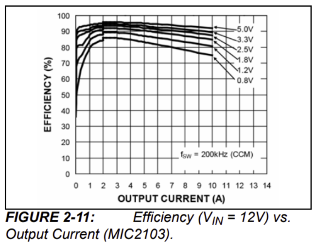
In addition to these benefits, this IC provides quite a high efficiency for higher output currents (~94%):
This controller is also readily available and can be obtained from most distributors such as Arrow, Digi-Key, Mouser, Farnell, etc. You can also buy this chip directly from the manufacturer. The price for this IC is low for a high current output controller. The manufacturer also supplies an evaluation board MIC2103YML-10A, which can be used as a reference design to help when making decisions in your PCB design.
Schematic Design
The schematic design of the MIC2103 DC-DC buck controller was relatively more complex than the previous design. Discrete component choices required a lot more calculations and design considerations.
The schematic design and the component selection were divided into the following steps:
- Output voltage calculations and feedback circuit
- Choice of switching frequency
- Circuit current limit choice
- External MOSFET selection
- Bootstrap circuit
- Inductor selection
- Input and output capacitor selection
- Snubber circuit
- Additional functions
1. Output Voltage Calculations and Feedback Circuit
For the first step of the schematic design, the calculation of feedback resistors was chosen because we need to ensure a stable 5 V output voltage for our supply design. The resistors were calculated using the following formula, which is given in the data sheet:

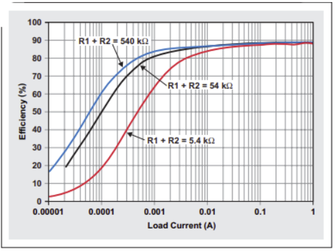
As discussed in the previous DC-DC buck converter design, there is a difficulty when the feedback decider circuit’s values need to be chosen. Low values would mean that the converter will be less efficient when light loads are connected. However, using this option, the converter would be less susceptible to noise. High values would have the opposite effect, as can be seen in the graph below.
An additional consideration is that choosing resistance values for the divider that are outside of the recommended range as specified in the data sheet can result in undesirable effects, such as a change in the output voltage due to feedback leakage current, as shown below.
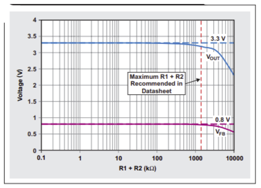
The output voltage accuracy will also depend primarily on the feedback circuit, so choosing precise resistors with <1% tolerance values is recommended to get the required results.
As this design is intended for use with higher loads, the feedback resistors that were considered are low values.
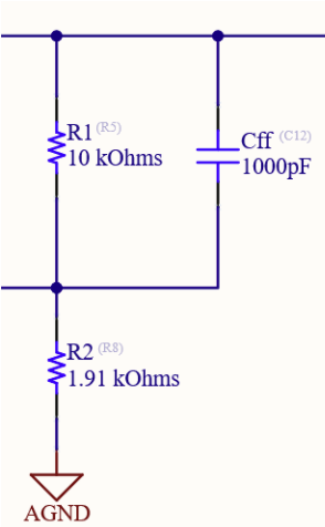
The data sheet suggests taking an R1 resistor value somewhere between 3 kΩ and 10 kΩ, and so, for this design, a 10 kΩ resistor was chosen. So now that we have selected the R1 resistor, this just leaves us needing to find the value of the R2 resistor using the equation below.

A feedforward capacitor with a value of 100nF has been added to increase the overall stability of the feedback circuit:
2. Choice of switching frequency
The MIC2103 controller has an adjustable frequency, which means we can set the required operation switching frequency using external discrete components. This is typical for many analog components: a voltage divider is used to drop down some voltage to a specific value, and this voltage is read into the buck voltage controller. The switching frequency can be adjusted between 200 kHz and 550 kHz by changing the resistor divider on the FREQ input: The frequency can be calculated using the following formula:

where:

For more precision, the value of R20 from this graph can be used:
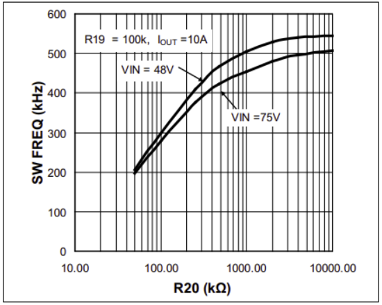
Selecting a higher switching frequency will reduce the required output capacitance and inductance values and reduce the actual size of output capacitors and inductors. But at the same time, the higher the frequency, the lower the efficiency becomes. For this design, a frequency of 300 kHz was chosen as we have sufficient available space for component placement, and we do not want to significantly reduce efficiency.
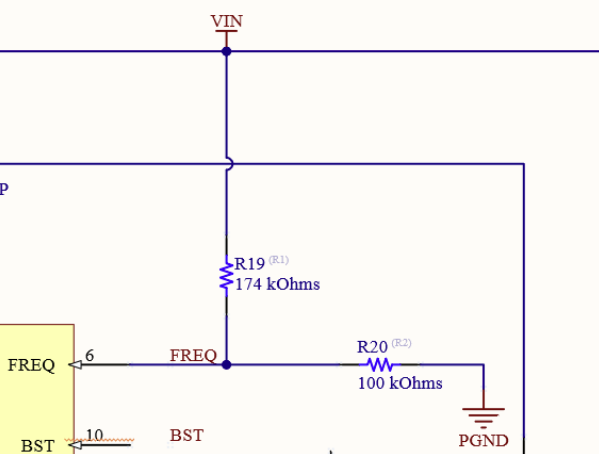
So, by choosing a frequency of 300 kHz from the graph above, an R20 resistor value of 100 kΩ was needed. As we now have the switching frequency we want and the corresponding R20 resistor value, we can calculate the one resistor that is left, which is R19, using the equation below:

3. Circuit current limit choice
As we are designing a switching voltage controller that can supply 6 A of output current, we do not want to exceed that limit by much more. This is because it could damage our controller, the voltage source, or even the load.
The current limit is set by a resistor, the value of which can be calculated using the following formula from the data sheet.

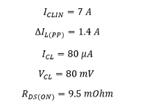
The current limit that was chosen is 7 A because we do not want to exceed the output current by too much, but at the same time, we do want our power supply to be able to generate the required 6 A of current and not to turn off if there are any small rises in output current caused by transient current spikes.

In addition, a parallel capacitor was connected to increase the accuracy of the current sensing circuit and provide more stable protection as it filters the switching node ringing during the off-time (prevents the current limit function from false activation). The capacitor value should be chosen so that the RC time constant would be much less than the minimum off-time of the IC.
The RC time constant can be easily calculated by using this formula:
Τ = C x R
Alternatively, a calculator can be chosen for this task. There is plenty of online calculators available, so do not be shy to use them as it can save a lot of time and sometimes prevents mistakes.
A small capacitor of 10 pF was chosen, and the time constant of the RC circuit was 0.00001s (10 µS).
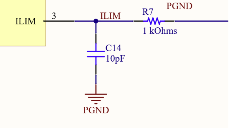
Also, this IC includes hiccup mode short circuit protection. This type of short circuit protection is very reliable because it shuts down the regulator IC if a short circuit is detected. When the short circuit condition is removed, the IC recovers and starts working again.
4. External MOSFET selection
External switching MOSFET selection was probably one of the hardest decisions in this design. You will find MOSFET selection is the most critical part of any DC-DC buck controller design using external switches. Firstly, these are parameters which should be considered:
- Gate-Source turn-on voltage
- On-resistance
- Total gate charge
- Capacitance characteristics
- Voltage rating
The MIC2104 controller operates using the input signal voltage to control an internal 5 V LDO, which provides power to turn on the high-side and low-side MOSFETs. So, when we choose to use a MOSFET as an external switch for this controller, we need to be sure that it completely turns on at voltages of < 5 V.
However, using a MOSFET with a Vgs that is too low can result in false switching, which can adversely affect the switching power supply output. From the data sheet, the recommendation is to use a MOSFET that is specified to completely turn on when Vgs is 4.5 V.
The MOSFETs selected for the high-side switch and low-side switch calculations were the DMN2011UFDE-7. This MOSFET is relatively compact and has a Vgs(on) of 4.5 V.
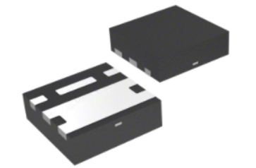
The other essential electrical characteristic of the MOSFET used in this application is the resistance between the source and drain when the MOSFET is fully open (On-resistance). The higher the on-resistance is, the greater the voltage drop will be between the source and drain, and consequently, a larger voltage drop will result in the need for more heat dissipation. Too high a voltage drop can cause MOSFETs to heat up, and in addition to that, it affects the controller’s efficiency. For this MOSFET, the on-resistance is 9.5 mΩ.
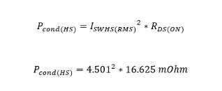
By taking the on-resistance and the maximum current we are using, we can calculate the maximum power dissipation for the MOSFETs.

High-side MOSFET:
While:
R(on) = 16.625 mΩ (Although the R(on) of the chosen MOSFET is 9.5 mΩ at 25 oC, during standard operation, the MOSFETs will tend to heat up and R(on) will increase, and the MIC2103 data sheet recommends increasing the nominal resistance by 75%)
Minimum and maximum duty cycle values were chosen to allow calculation of the maximum power dissipation that can occur at the rated specifications of the designed power supply.
Minimum duty cycle:

Maximum duty cycle:

Current and power required to turn the high-side MOSFET on:


Current and power required to turn the low-side MOSFET on:

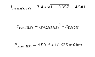
The calculated maximum power dissipation for the MOSFET is 0.4655 W, and the specified maximum power dissipation for the chosen MOSFET is 0.610 W.
The other characteristic is the total gate charge. The total gate charge is the charge that is required to turn the MOSFET on and off. The gate drive circuit supplies the gate charge for the MIC2103.
The current required to turn the high-side switch on can be calculated using the formula:

From the formula, we can see that the lower the total gate charge is, the better this will be as it will require less current to turn the MOSFET on and off, and therefore increase the efficiency.

For the low-side switch, the gate drive current can be calculated by using the input capacitance Ciss characteristic at Vds = 0 instead of the gate charge for a more accurate result:


The total power requirements for the gate drive can be calculated by using the following formula:

The voltage rating of the MOSFET also should be considered. It is recommended that a MOSFET is used that has at least 20% higher Vds(max) than the input voltage in case there are any voltage spikes caused by parasitic circuit elements. As we are designing a power supply with a maximum input voltage of 14 V, it is not difficult to find MOSFETs that can withstand such voltages. The Vds(max) of the chosen MOSFET is 20 V.
5. Bootstrap circuit
A bootstrap circuit is required because we are using an N-channel MOSFET, rather than a P-Channel, as the high-side switch. This circuit has a diode and a capacitor connected in series:
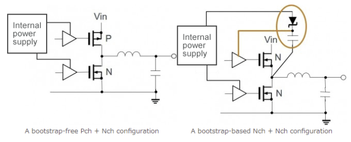
For the diode selection, a simple signal Schottky diode (type BAT46W-TP) was used. It is cheap and relatively compact. Also, this particular diode was recommended in the design of the MIC2104 evaluation board. The capacitor is typically 100 nF .
6. Inductor selection
In common with the MOSFET selection, the inductor selection for high current switching power supplies is critically important.
First of all, we need to calculate the required inductance for our switching supply using the following equation:

The chosen current ripple for this calculation was selected to be 20%, as this is the recommended value in the data sheet. Note that this ignores the voltage drop across the MOSFETs, which is generally small enough to ignore at the voltages we're looking at here. Many data sheets recommend choosing the current ripple value to be somewhere between 20% and 30% of the output current.

Now that we have calculated the inductor value of 7.65 uH, we can choose the inductor. An inductor with this specific value that was also rated for the required high current was not found in the product library. Therefore, a Bourns SRR1280-6R8Y inductor with a value of 6.8 uH was chosen as the best and closest match.
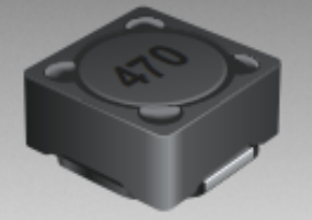
This inductor has a current rating of 7.6 A and a saturation current of 8 A. It is essential that these inductor parameters are higher than the peak current that we want to draw from our power supply.
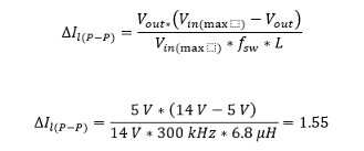
Now that we have chosen the inductor, we can calculate the inductor’s peak to peak current and peak current using the equations below.
Peak to peak inductor current:
Peak inductor current:
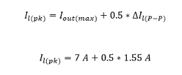
With these currents, we can then calculate the power dissipated by the inductor:
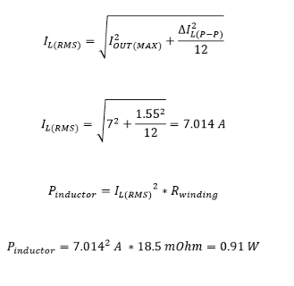
7. Input and output capacitor selection
Input and output capacitors are also critical components for any switching power supply, as they provide noise filtering and the bulk capacitance for energy sourcing and decreasing the voltage ripple.
The input and output capacitor values have been selected from the data sheet recommended design. It was seen that our requirements were quite similar to those that have been used in this design. The only difference is that instead of the 6 A output current, a value of 10 A has been used:
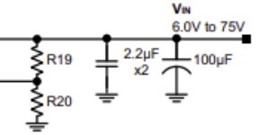
However, instead of using one big 100 uF capacitor, two 68 uF SMD electrolytic capacitors were used for the buck capacitance. Also, three 2.2 uF X7R ceramic capacitors were used for noise filtering and to decrease the total ESR value of the input capacitor network.
Nevertheless, for the selection of the input capacitors, it is not only the value of capacitance that is important, but other parameters are also very important, including:
- Ripple current rating
- ESR
- Voltage rating
First, we need to calculate the input ripple current rating using the following equations:
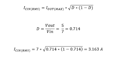
Then we need to calculate the power which will be dissipated through the capacitor, which is calculated as follows:

To calculate the dissipated power, we first need to determine the total ESR for the input capacitors.
The ESR value for the selected electrolytic capacitors was found in the data sheet and is 440 mΩ. However, the ESR value for the selected ceramic capacitors was not clearly defined. So, the impedance graph from the relevant capacitor page was taken, and the resonance frequency was chosen so that we can see the minimal impedance value, which is the DC resistance or ESR value of the capacitor.
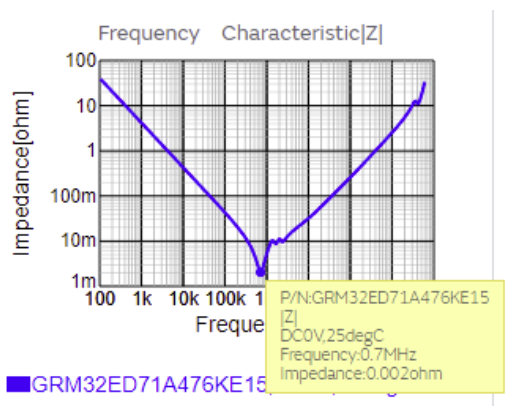
We can now see that each ceramic capacitor has an ESR of 0.002 Ω or 2 mΩ.
The total ESR value of the whole network can now be calculated using the parallel resistance formula, or alternatively, you can calculate this using an online parallel resistor calculator.
We can now see that the total ESR of the input capacitors is 0.66 mΩ.
Using this value, we can measure the total maximum power dissipation for the capacitors:

And also, we can calculate the input voltage ripple:
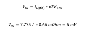
For the voltage rating, we must choose the right type of capacitors. If you decide to use tantalum capacitors, you need at least double the voltage rating than the maximum input voltage. In contrast, it is sufficient for the voltage rating for electrolytic capacitors to be just 20% higher than the maximum input voltage.
For the output capacitors, the reference data sheet design was used again to choose these.
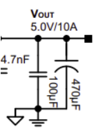
The only difference is that instead of using an expensive 100 uF ceramic capacitor, two cheaper 47 uF capacitors were used.
First, we need to find out the total ESR of the output capacitor network.
The ESR of the electrolytic capacitors is defined as 160 mΩ. The ESR of the ceramic capacitors is defined as 10 mΩ.
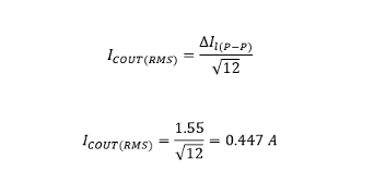
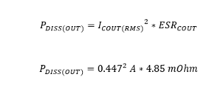
Now that we know the total ESR of the output capacitors, we can calculate the output ripple voltage, the RMS output current, and the maximum power dissipated by these capacitors using the following equations.
Output voltage ripple:
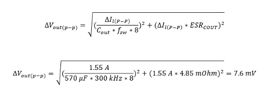
RMS output current:
Power dissipated by the capacitor leads at maximum current output:
8. Snubber circuit
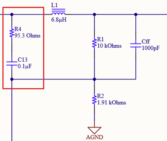
The snubber circuit is used for voltage ripple injection into the IC’s feedback pin to increase the output voltage’s stability. The values of the required capacitor and resistor can be calculated using the formula from the datasheet; however, in this case, the recommended 100 nF ceramic capacitor and 95.5 kΩ resistor were used because of the conditions of the feedback circuit in the suggested design is the same as our design.
9. Additional functions
The switching buck voltage controller has the following two additional functions:
- Power Good (PG) - this function indicates when the device has managed to regulate its output to the desired output voltage. It indicates that the power rails are stable and can be used in situations where more than one regulator is used in the power supply.
- Enable (EN) - this function allows the power supply activation and deactivation by using an MCU, voltage supervisor, watchdog IC, or a simple transistor or logic network.
As this design is for a standalone power supply, these functions are not required and are put in the appropriate default state by pulling high the pins in the circuit using pull-up resistors.
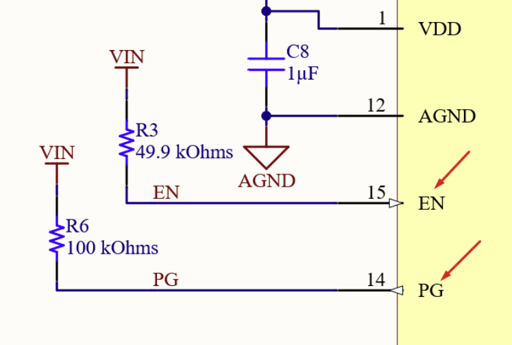
Now we can finally see the entire schematic of the designed DC-DC buck controller power supply using our calculated values:
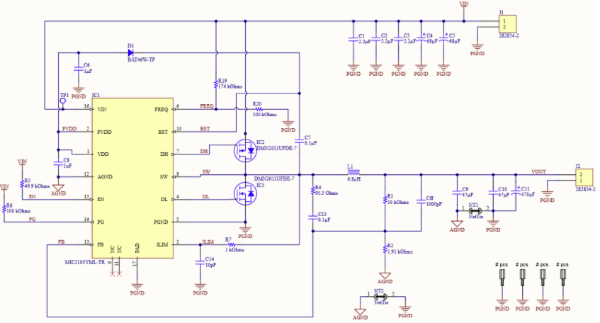
Schematic design simulation
Now that the circuit design has been completed, it is good practice to simulate the circuit whenever possible. For the MIC2104 DC-DC buck controller, Microchip has provided simulation files which can be opened using the “SIMPLIS” power and analog circuit simulation software while using Microchip’s “MPLAB” extension.
You can download a free SIMPLIS demo version from here:
https://www.simetrix.co.uk/downloads/download-elements.html
This free demo version has some design and simulation functionality restrictions, but it works great for this design.
You can download the free MPLAB extension from here:
https://www.microchip.com/mplab/mplab-mindi
After you have downloaded and set up the program, some previously made simulation files can be found here:
https://www.microchip.com/SWLibraryWeb/product.aspx?product=AnalogSimMIC2103
After finding and downloading the pre-made MIC2104 DC-DC buck controller design, changes can then be made corresponding to our designed schematic, as shown below.
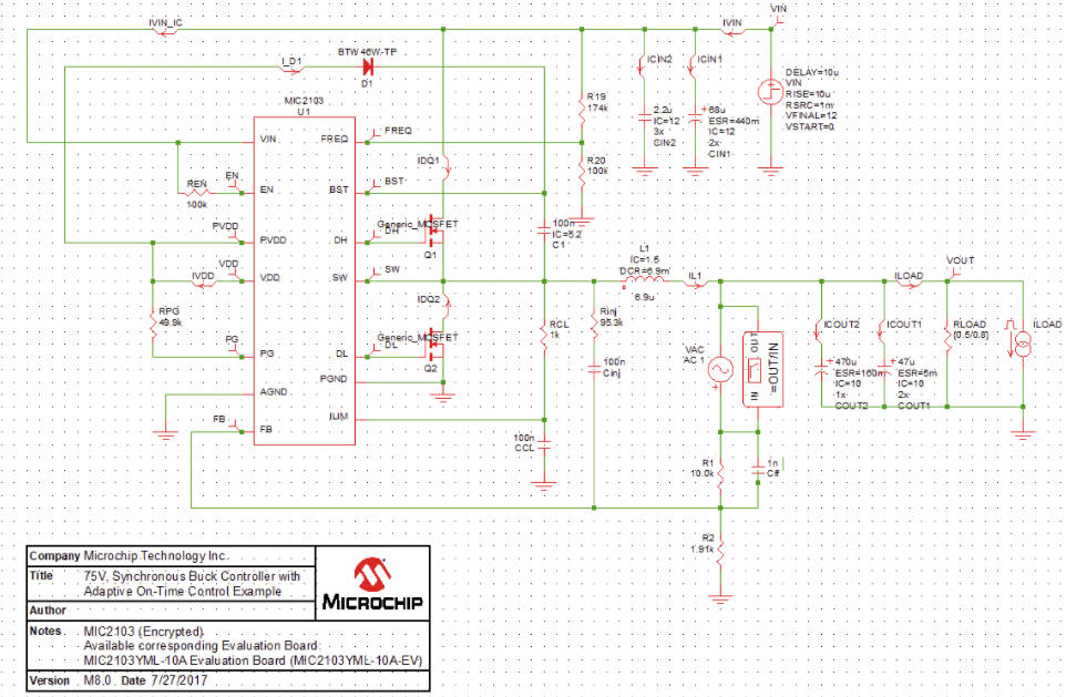
Now that the simulation circuit has been completed, it is possible to calculate parameters including the controller’s start-up time, AC transient response time, output voltage ripple, etc.
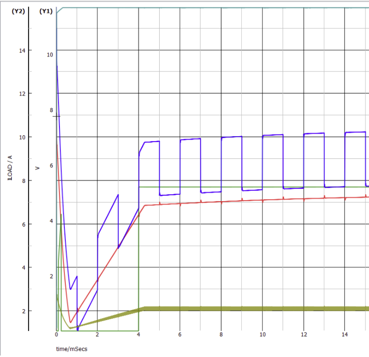
As we can see from the simulation, the IC has a soft start function that enables the circuit to start operating after a delay of 4 ms by holding the Enable pin (Green) LOW for this time.
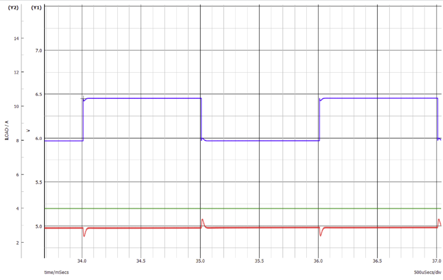
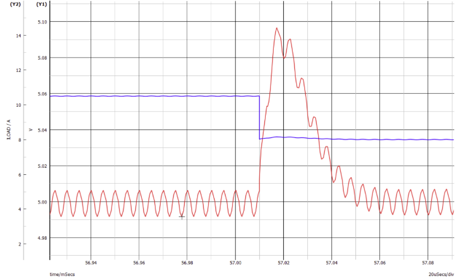
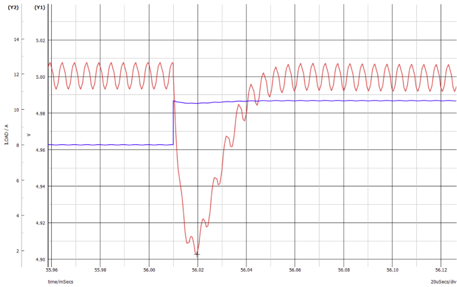
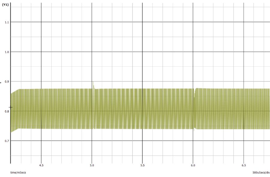
Simulating the feedback pin voltage is a good way to select the best feedforward capacitor value as the data sheet suggests a pretty wide range of values from 1 nF to 100 nF. Choosing the right value is very important as it directly influences the output voltage ripple.
Performing circuit simulation is a great way to try out your designed circuit and discover what power supply parameters influence the components. I made sure my graduate engineer fully understood the implications of modifying values as part of the teaching exercise. Also, by observing the effect due to the absence of one or more recommended components, you can find how much they affect the operation.
PCB Layout
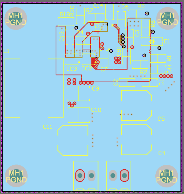
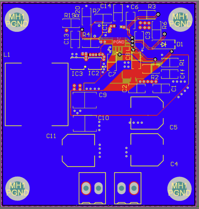
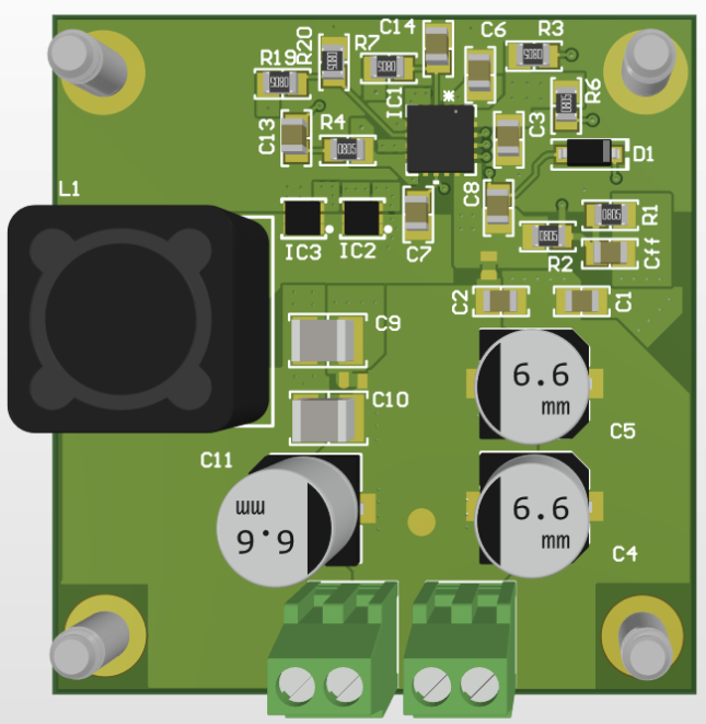
For this design, you will see that the corresponding PCB layout was way more complicated than for the previous DC-DC buck converter. This is because having a high current, such as 6 A, in this case, will require accurate component placement, more complex thermal considerations, wide traces, separated analog and power grounds, and four layers.
For the PCB layout, the recommended design for the evaluation board (MIC2103YML-10A-EV) was used as a reference.
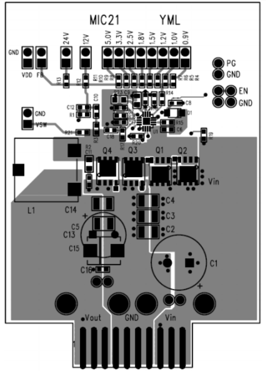
The first step in the PCB layout for this high current buck converter is component placement.
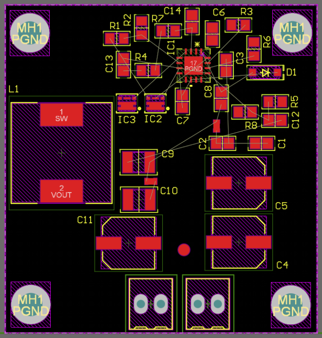
There are some general guidelines which need to be considered for the placement of the components:
- Place the input capacitors on the same side of the board as MOSFETs.
- The 1 µF ceramic capacitors connected to the VDD and PVDD pins must be located close to the IC. The VDD pin is very noise sensitive, and the placement of the capacitor is very critical.
- Place the RC snubber on the same side of the board and as close as possible to the SW pin.
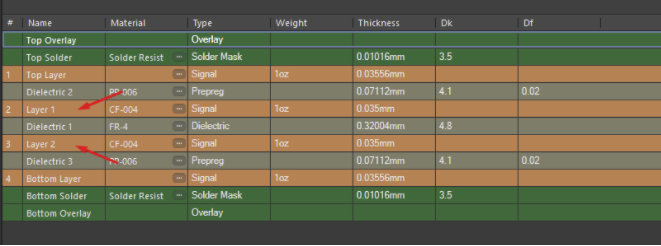
As a second step, add inner layers to the PCB, and this design requires at least 4 layers:
Top Layer - Power, Signal, Ground
1 Layer - Whole layer dedicated to Ground
2 Layer - Power and Ground
Bottom Layer - Power and Ground
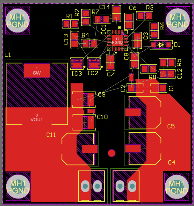
As a third step, polygons for the input and output voltage tracks were made as wide as possible to ensure they have sufficient current flow capability.
Also, care should be taken of other important traces such as SW, DL, DH, and FB.
The data sheet also provides the following PCB layout guidelines:
- Keep the inductor connection to the switch node (SW) short.
- Do not route any digital lines underneath or close to the inductor.
- Use a wide trace to connect the output capacitor ground terminal to the input capacitor ground terminal.
- Signal and power grounds should be kept separate and connected at only one location.
- Keep the switch node (SW) away from the feedback (FB) pin.
After careful routing following all the guidelines, the PCB looks like this:
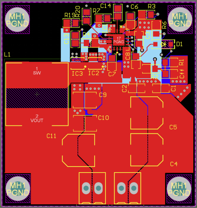
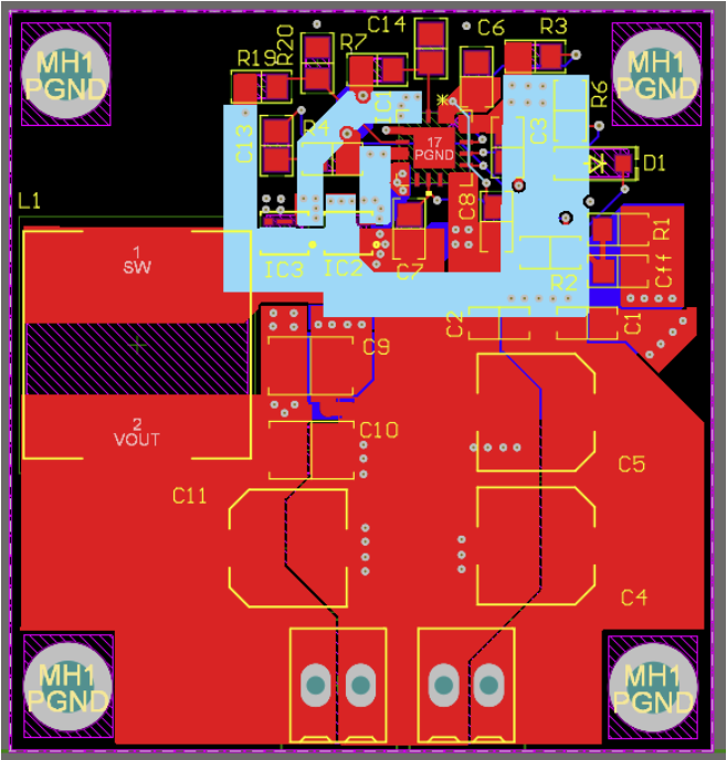
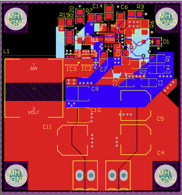
And the last step was to add a whole GND plane to one inner layer and GND polygons to the remaining areas of the other layers:
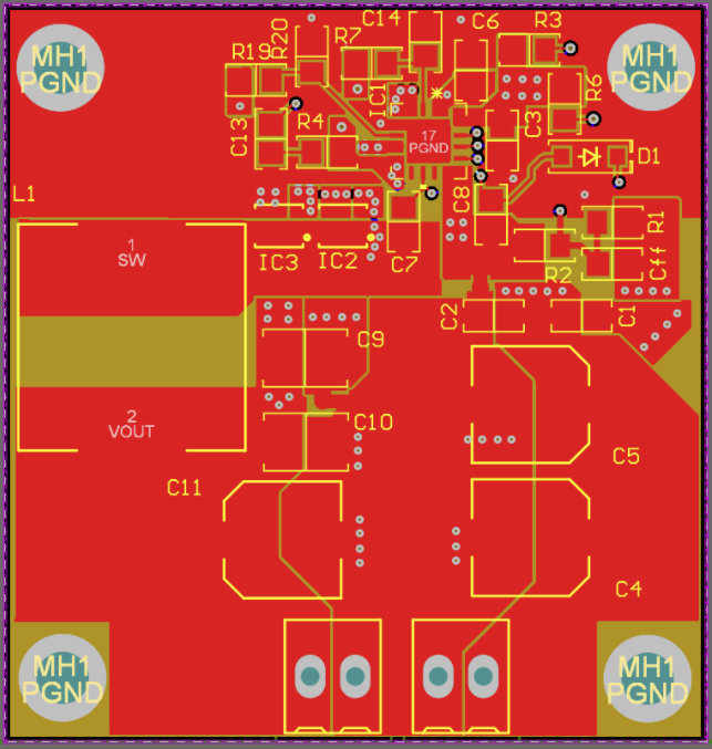
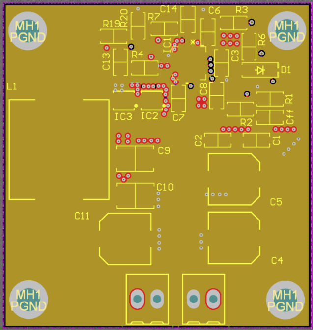
PND Analyzer
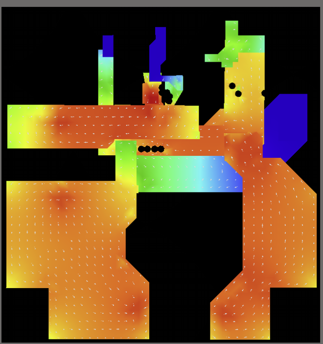
The Altium tool called “PND Analyzer” is an extremely useful tool for power supply design. The current path from the inputs to the outputs for this design was simulated using the PND Analyzer.
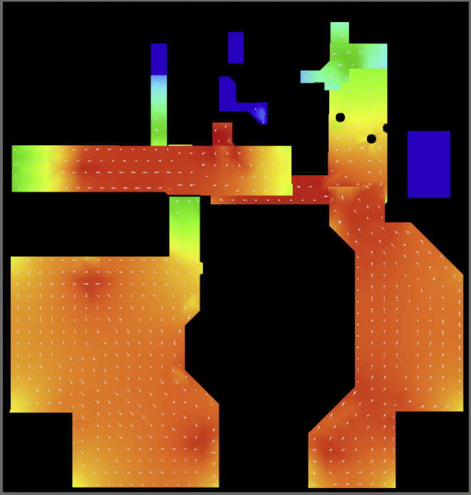
The RED colored areas indicate where the current peaks are at their highest, while any BLUE areas are regions where there is no current flow at all. Note that we cannot take the BLUE areas into consideration at this time, as not all the possible scenarios have been stimulated during the simulation.
However, we can already see that there are several RED regions where the current density can cause thermal problems as a result of our design. These will need to be addressed.
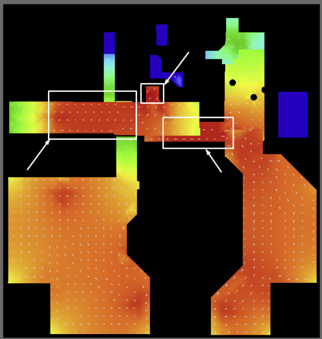
These marked places show where your components and the PCB can significantly heat up over time when the power supply is on a continuous load. This especially applies to the MOSFET’s mounting location and the heat that they generate due to their ‘on’ resistance. Increasing temperatures will cause an increased voltage drop, causing them to generate even more heat. This thermal loop could cause fatal problems.
To address these issues, small corrections to these polygons have been made.

Although some regions are still left with a relatively high current density, you will see that these areas are now better distributed across the PCB.
Conclusions
The design of the 30 W (5 V output voltage and 6 A output current) high current buck converter design has much greater complexity than for the simple low current regulator. This is because of a range of factors, including the need to take into account thermal capability, the complex calculations, the choice of external switches, and the necessity for wide polygons instead of narrow traces that this design required. There are a few points to summarize here:
Calculations for component selection
During the schematic design, many calculations are required. These can take some time, but they’re really worth the effort. By doing the math yourself, you can really start to understand how the controller works, how to choose components, and which parameters are more critical and which are less critical. Input and output capacitors, inductor selection, external switch (MOSFET) selection, feedback circuit design, frequency selection, and current limiting, all these functions were included in this design. You will find all of them are critical for the stability and reliability of the finished power supply.
Also, as this IC’s data sheet has fewer recommendations and more formulas, this has the advantage of giving you the freedom to choose your components. You can use different combinations of components to allow you to pick and choose power supply stability, output voltage, EMI/EMC compatibility, power integrity, physical size, price, availability, and so on.
The importance of simulations
Undertaking a simulation of the schematic design is also very advantageous if it is possible. The more you can simulate, the better. You can try different components and see how this affects performance. For example, it may be hard to find an inductor with the required inductance and current for a low price, so choose one with a different inductance and then simulate it to see what difference it makes. Alternatively, how about changing the capacitance and ESR to see how it will affect your power supply stability. Just don’t forget that although some simulations are very accurate, they can’t simulate precisely how your device would work in the real world as there are simply too many variables to consider.
For a higher power design such as this, the PCB layout is also extremely important. You need to consider component placement very carefully and know where the highest current will flow. Then there are other considerations such as the need for wide VIN, VOUT, and SW traces (and where it’s better to place a polygon) and the routing of other sensitive traces like Feedback. Also, there’s the placement of capacitors and the inductor, the need for separate power and analog ground plane, etc.
Thermal considerations
For current density considerations and thermal management, the PND Analyzer can be a great friend. By looking at your most important current path, you can see the current density across your PCB and make any corrections to eliminate hot-spots, which could be fatal once you have ordered and assembled the power supply. And if it is your first high power circuit design, there will be some for sure.
To sum everything up, this project took a lot more time, but I believe it was totally worth it. Component choice and PCB layout following all the calculations and guidelines were not easy; however, the SIMPLIS simulations and the PND analyzer were a huge help. Such projects can significantly increase a student’s or junior engineer’s competency as they will increase their component selection knowledge and teach them about controller characteristics, PCB layout, and thermal management. The theory is essential, but only when you begin to apply theoretical calculations into practice will you understand why they are crucial and the best ways to employ those calculations in your designs.
You can find the design files for many of my projects released under the open-source MIT license on GitHub. You’re free to use any of the circuits or projects as you wish, even for commercial projects. You’ll find details of the devices that we discuss in my massive open-source Altium Designer Library®. You’ll also find details of a huge range of different components contained in this library as well.