Best Practices for Using Reference Designs

Some designers love reference designs and some designers hate them. No matter how you feel about reference designs, the best component companies will release reference designs for their new and legacy products to show designers an example application for a component. Some reference designs are very high quality and could be easily adapted into a production-grade systems. Other reference designs are only good for the BOM and block diagram, leaving you to do the majority of the engineering.
Whenever my team needs to build a new type of application or we’re working with a component we’ve never used, I always go out and see if there is a reference design for that component or system. The goal isn’t to simply replicate the design into a new system. For me, it simply cuts down my research time: I can quickly see what major components are involved in the system and I can get a good idea of how they fit together at a high level. There’s always some additional requirement that needs to be engineered into the schematics, but the reference design still gives a good idea of how these additional features will fit into the design.
If the reference design is good enough and it very nicely illustrates how to quickly engineer around a few main components, I’m likely to use them in the design and the component maker has just earned my business. If you’re a newer designer and you’re wondering whether reference designs are right for your next project, follow these best practices so that you don’t make any mistakes with your reference design.
How to Use Reference Designs
There are different ways to find and use reference designs for PCB projects. Reference designs are created to show how a specific component or a line of components will be used for a specific application. These designs will usually include the following items:
- Block diagram, BOM, and schematics: This is the most important part of a reference design as it shows you how the main components are connected and what other components are needed for the specific application.
- PCB layout files: Not all reference designs will include a PCB layout, but those that do were probably manufactured and tested as a demo product at some point.
- Design libraries: Reference designs will include libraries with eth symbols and footprints for components in the design.
- Fabrication files: You might find Gerbers or other fabrication files in a set of reference design files.
Once you get the design files, there are a few tasks you should perform before your incorporate sections from the reference design into your custom design.
Check for Obsolete/NRND Components
If you download an older reference design, it’s possible that the design includes components that have gone NRND or are obsolete. Be sure to go through the design and check for any of these components and update the design with new parts. Your supply chain tools in your PCB design software should show you which components are NRND, obsolete, or unsourceable.
Check All Component Symbols and Footprints
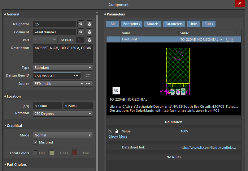
After you’ve replaced the outdated components, you should check the remaining components for any errors. Just because a reference design was created by a big component manufacturer doesn’t mean the libraries don’t have incorrect library data. I’ve seen reference designs from major component manufacturers with many incorrect symbols and footprints. All symbols and footprints should be checked to ensure the footprints match the part numbers in the design.

Keep the Schematics Organized
If you’re adding more functionality to a reference design, you should try to keep the schematics. This might involve separating circuit blocks from the reference design into different sheets or building out hierarchical schematics. I prefer to keep the reference portions in their own sheets and the newer circuit portions in their own sheets. A little work on the front end helps you identify bugs in the design and trace them back to the reference vs. custom design files.
Evaluate the Design with Simulations Where Possible
If possible, evaluate the design’s functionality with simulations. Doing this in the schematic is good enough as you’ll probably end up using a totally different layout anyways. One way I will do this is in blocks: I’ll look at specific blocks in the design with SPICE simulations and make sure they produce the electrical behavior I expect.
How You Probably Shouldn’t Use Layouts in Reference Designs
I prefer to use a reference design for the schematics and BOM, but that’s about it. I would not recommend taking the PCB layout and trying to adapt it to your own design. You can certainly look at the layout to get some ideas for how to arrange components, and you might be able to copy a few circuit blocks between the reference PCB and the new PCB, but that’s probably it.
Here’s why I would not recommend using the PCB layout in a reference design:
- Form factor: The PCB layout likely isn’t arranged to meet your form factor requirements and may not accommodate placement of other critical components that were not part of the original reference design.
- SI/PI: There might be some signal integrity, power integrity, and EMI problems lurking in the PCB layout. Some prominent names in the EMI/EMC crowd shun application notes and reference designs for precisely this reason: the component makers are not board designers and might make recommendations that create problems in the system.
- Testing: It may be impossible to know if the design was ever tested and what level of testing was applied. This is a major reason the layout in a reference design should be scrutinized.
- FCC, UL, or other certification: If you’re developing anything that requires some testing and certification, you’ll have no guarantee that the PCB layout in the reference design will receive certification.
Sometimes, the PCB layout in a reference design is just messy. While it might work at a functional level, the layout is normally just created as an example, and it would require major changes before it can be made ready for a production-grade system.

If you need to find a reference design, just hop over to your favorite search engine and start searching for your application. You’ll likely find multiple options from different component companies. The designs could be in any format, but the conversion tools in Altium Designer® let you take any reference design and get started with a new project. The component tools also help you find and place new parts in your designs with verified symbols and footprints.
When you’ve finished your design, and you want to release files to your manufacturer, the Altium 365™ platform makes it easy to collaborate and share your projects. We have only scratched the surface of what is possible to do with Altium Designer on Altium 365. You can check the product page for a more in-depth feature description or one of the On-Demand Webinars.
