Instantly Check Every Copper Connection With Rules-Driven PCB Design Tools

It’s easy to find errors in most simple PCBs. Simply scan through your critical nets and trace each copper connection from source to load. Today’s printed circuit boards are not so easy to inspect and validate by eye. Even relatively simple low-speed boards can have hundreds of components packed into a small space, and it’s easy to get lost in a complex PCB layout.
Today’s modern designs demand modern design tools. Altium Designer users have access to a range of design tools that run on top of a rules-driven design engine. These tools automatically check a PCB layout against design rules as it’s created, allowing every incorrect copper connection to be spotted instantly as it’s created in the PCB. When you need to create an accurate circuit board layout and ensure it can be manufactured correctly, you need the rules-driven layout features in Altium Designer.
ALTIUM DESIGNER
The only PCB design package built on a unified rules-driven design engine.
Keeping track of every copper connection in your circuit board layout can be a difficult task, especially in a complex board. A simple board can usually be scanned by eye, while complex boards need some automation to pass evaluation and reach signoff. For this reason, designers need the ability to define a complete set of design rules in the PCB design software. This will help them catch a range of errors, such as clearance violations, net errors, and incorrect copper connections.
Whenever there is an incorrect copper connection, PCB layout tools should flag the error early in the design in order to minimize the amount of rework. The best PCB design software runs on top of a DRC engine, which will check the circuit board layout against standard and custom design rules. With this set of tools, designers will have the ability to check every copper connection and correct any mistakes before sending a board out for PCB fabrication and assembly.
What Happens When Copper Connections Go Wrong?
Whenever there is a mistaken copper connection that makes its way into a finished board, several problems can occur. Some of the common problems include:
- Short and open circuits: The most common problems that arise from an incorrect copper connection are open and short circuits. Mistaken bridging or incomplete routing need to be flagged during design.
- Incorrect component and net connections: Sometimes, a copper connection that was correct now becomes incorrect when a component is moved. The new copper connection on the board surface or internal layer may no longer reference the correct net, and signals in the board will not be routed to the correct components.
- Manufacturing mistakes: If a short or open circuit is missed in the design, the mistake will be reflected in the copper regions in your Gerber files. As a result, critical circuits may not work properly after PCB fabrication and assembly, and you’ll have wasted a board spin.
Spot Copper Connection Errors in Design Rule Checks
The time to spot copper connection errors is as soon as possible. In the PCB layout, spotting these errors early ensures your design will work properly once you go to manufacturing. With the right set of layout tools that interface with your PCB design rules, it’s easy to prevent copper connection errors and fix them should they occur.
- Your design rules should be formulated using the best PCB design guidelines for any board, as well as some specific guidelines for your particular application.
- A cramped PCB layout creates the risk of short circuits between nearby components, but setting clearance rules helps you prevent unintended copper connections.
Learn more about setting trace and pad clearance rules to prevent shorts.
- Advanced boards like HDI designs can be at major risk of bad copper connections if design rules aren’t set up properly.

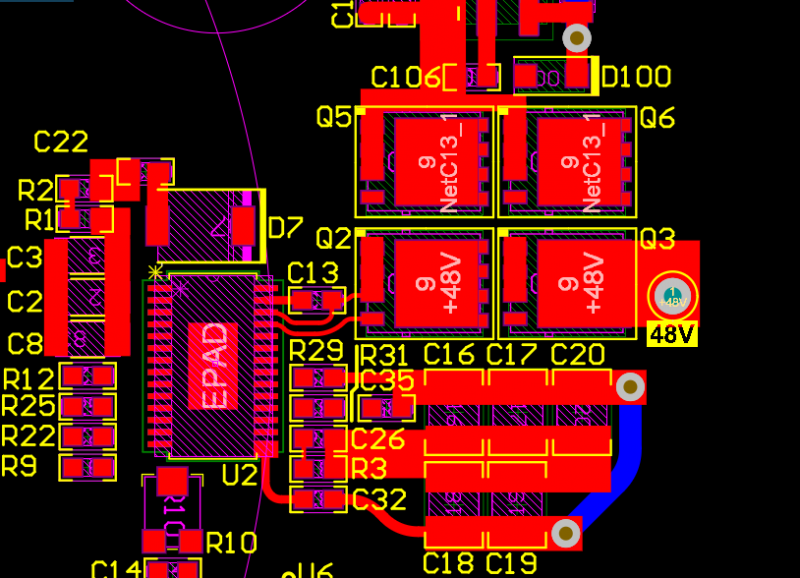
There is a risk of unintended copper connections in this cramped circuit board layout. Altium Designer can flag potential problems early in the design process.
Create Interconnects With Powerful PCB Layout and Routing Tools
As you create your PCB layout, you’ll need to do more than just place traces and components. Routing through vias and between plane layers is commonplace in modern PCBs. Anytime traces, vias, pads, or holes are placed in a PCB layout, bad copper connections from bridging need to be checked. As part of routing, this ensures signals get to the intended destination and that there are no shorts in the circuit board layout.
The Best Routing Tools Prevent Bad Copper Connections
Routing tools that run on top of a rules-driven design engine will help you prevent mistakes in your PCB layout, and they can ensure your next design complies with important signaling standards. Low-speed and high-speed designs can have the same risk of open and short circuits during routing, but rules-driven routing features will check for these errors as traces are routed in the PCB layout.
- Whether you’re designing a simple low-speed board or an advanced impedance controlled high-speed PCB, powerful routing tools can help you define copper connections while preventing mistakes.
Learn more about important rules and constraints in high-speed PCB routing.
- Keeping traces separated during routing is all about preventing crosstalk and bridging during assembly.
Learn more about setting your required trace spacing for your circuit board layout.
- Even if you set proper clearances between copper elements to prevent bridging, you’ll still need to keep extra clearance when working with high voltage design.
Learn more about defining clearances between conductors in your high voltage PCB.

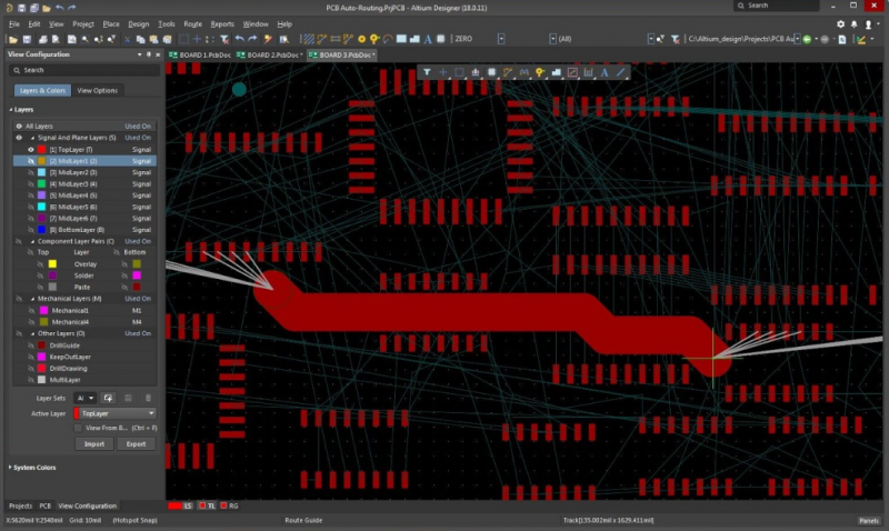
You can navigate a complex PCB layout without bad copper connections thanks to the rules-driven design engine in Altium Designer.
Altium Designer Spots Invalid Copper Connections Automatically
Altium Designer is a unified rules-driven PCB design platform that makes the most advanced design and layout tasks easy. The rules-driven design engine in Altium Designer helps you layout components, route traces, specify planes and vias, and set 3D models for components in a single program. All the design rules you define will be checked as you create your PCB, including required clearances for copper connections between components, pads, vias, traces, and planes. Instead of inspecting your board manually, you can stay productive and prevent design errors when you use Altium Designer.
The Power of Rules-Driven Design in Altium Designer
The rules-driven design engine in Altium Designer does more than just spot open and short circuits, it interfaces with all your important design and layout tools. Every aspect of your circuit board layout can be inspected automatically as you create your design. The design rules you create can be adapted to any application, including high-speed digital designs, high voltage equipment, and high-frequency analog systems.
- Altium Designer makes checking for copper connections leading to shorts or opens extremely simple. The online DRC engine will examine your board as it’s created, and you can run DRCs anytime during design.
Learn more about the rules-driven design engine in Altium Designer.
- The MCAD design environment in Altium Designer will also show you copper connections in 3D, allowing you to see how every component, trace, via, and plane is connected in your PCB layout.
- Once your design is complete and has passed all rule checks, you can instantly share your design data in the cloud using the Altium 365 platform.

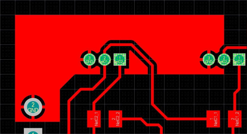
The DRC engine in Altium Designer instantly flags invalid copper connections in your PCB layout.
You don’t need to manually inspect every copper connection and interconnect in your circuit board when you use a complete set of rules-driven design tools. Keep yourself at the cutting edge and at your most productive with the powerful set of design tools in Altium Designer.
Altium Designer on Altium 365 delivers unprecedented integration to the electronics industry until now relegated to the world of software development, allowing designers to work from home and reach unprecedented levels of efficiency.
We have only scratched the surface of what is possible to do with Altium Designer on Altium 365. You can check the product page for a more in-depth feature description or one of the On-Demand Webinars.
