Identifying Minimum PCB Trace Spacing and Width in Altium Designer

Taking the time to set up routing rules to govern the minimum trace spacing and trace width for PCB layout can be tedious. Many designers would prefer to jump in and start trace routing without going through this setup process first. This can be dangerous though as you may inadvertently route a trace routing at the wrong width, or pack your routing in so tightly that you don’t have the room to make any width corrections later on. The more rigid the design requirements, the more dangerous this can be, even to the point of forcing you to re-do major sections of your routing in order to meet your design requirements.
The CAD tools in PCB design software have been set up to help you create your routing rules, and these capabilities have been around for a long time. However, you need to configure routing rules for your specific application as minimum trace spacing and trace width requirements can be very different in various applications. Fortunately, PCB design software has tools and resources that make the job of setting your routing rules up a lot easier than it used to be. Let’s look at what it takes to set up your routing rules and trace spacing in Altium Designer®.
What is the Minimum Trace Spacing and Width?
There are many rules that relate to routing and trace sizing in PCB design. Different rules become quite important in different applications, and designers should take time to understand these various rules when preparing a new design. Two common cases where you need to specify minimum trace spacing and width together in a design are:
- High speed design. A common rule of thumb is to set the minimum spacing between single-ended traces as triple the width of the traces. The goal here is to limit crosstalk, but this rule of thumb was developed at a time when crosstalk was much lower. Fast rising edges can create crosstalk, and you should always verify the required trace spacing with simulations or measurements.
- Differential pair routing. When you need to route differential pairs, you need to maintain specific spacing between each end of the pair. This is done to ensure the two pairs maintain consistent differential impedance.
- High voltage design. In high voltage design, an electrostatic discharge can occur between two conductors when they are placed to close together. To prevent discharge, determine the required minimum trace spacing under the IPC 2221 standard before creating your PCB layout. As high voltage designs could also be high current designs after power conversion, it's important to look at the minimum trace width as well, which can be determined fromt he IPC 2152 nomograph for high current designs.
In some cases, such as low-voltage slow-speed digital designs that don't need impedance control, you won't need to worry about a minimum trace width, and you'll probably have some freedom on spacing. DFM requirements can also place very close limits on your trace spacing.
There are two ways to enforce minimum PCB trace spacing and trace width routing rules in Altium Designer. The first is to specify the nets you want in each individual rule. This works well when you are working with a single net, but requires the use of the “Rule Custom Query Builder” when more than one net is being assigned.
The other method to identify nets for net rules in Altium Designer is to create net classes and then assign those classes to the routing rules. The net class tools allow you to point and click which nets that you want to assign. Also, the net class assignments can also be passed into the layout from the schematic. Working with a net class in Altium Designer’s layout editor is the method that we will focus on here.
To work on the spacing, open up the Printed Circuit Board PCB panel if it isn’t already opened and make sure that the main category is set to “Nets” at the top. If you already have some net classes identified, the PCB panel will look similar to the picture below.
The PCB panel “Nets” in Altium Designer
Before you route the next group of nets in your layout, you'll need to make sure you apply the minimum trace spacing rule to all required nets. The easiest way to do this in a complex layout is with a net class.
Creating a Net Class for Your Design Rules
Creating a net class gives you a quick way to assign a single design rule to multiple nets at once. This is a great way to quickly apply a single design rule to 100's or 1000's of nets. We are going to create a net class named “Test” which as you can see in the picture above does not yet exist. To create this net class you must first add a new net class by right-clicking in the panel as you see in the picture below.
Adding a net class in Altium Designer
By clicking on “Add Class” you will open up the “Edit Net Class” dialog box as you can see below. On the left side of the picture you can see where we have added the net class name of “Test”. We have also selected the nets that we want in our net class. To select a range of nets select the first net, and then while holding down the shift key select the last net.
Adding nets to the new net class
On the right side of the picture above we have used the single arrow key to send our selected nets from the “Non-Members” category to the “Members” category. This completes our net class, and by clicking OK our net class will be saved.
Net classes have a lot more uses then just for setting up design rules. In the picture below you can see the “Test” net class that we just created in the list of net classes. We have also selected that net class and you can see how the nets of that class have been highlighted. When selected, Altium Designer will zoom into the nets of the net class that are highlighted giving you another very valuable tool to use while you design and solder your board.
Selecting nets in Altium Designer by using the net class
Creating a Routing Rule for Trace Widths
Now that we’ve created a net class of the nets that we want to assign specific routing rules to, it’s time to create those rules. In the “Design” pulldown menu, click on “Rules” to open up the “PCB Rules and Constraints Editor”. We are going to create a new “Width” rule among the other rules for polygons, pads, and vias that you can see are already defined in the picture below.
Adding a new routing width rule in Altium Designer
Position your cursor over the Routing > Width rule as you see above, and right click your mouse. In the small pop-up menu, select “New Rule”. This will create a new rule and display its details as you can see in the picture below.

Assigning a name and the object match to the new rule
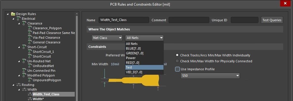
You can see above that we’ve given our new rule the name of “Width_Test_Class”. Right below that is the “Where The Object Matches” section where you will identify what the rule will be attached to. In the first drop-down menu you have several choices of categories to choose from:
- All (nets)
- Net (single)
- Net Class
- Layer
- Net and Layer
- Customer Query (multiple nets)
In our case we selected “Net Class” in order to use the net class that we created above.
The second drop-down menu is context sensitive and will display the options for whatever category you chose in the first drop-down menu. Since we chose net class, the second drop down menu displays for us a list of the different net classes that we can select. In our case we selected the net class that we created above named “Test”.
Finally, the third dropdown menu allows you to select an impedance profile if one is required for your design. As was mentioned above, impedance control is needed when you have a high speed or high frequency board, and when you're routing differential pairs. Altium Designer lets you create an impedance profile in the Layer Stack Manager, and you can set it in the design rules window shown above. Note that this will only enforce a trace spacing if you're working with differential pairs.
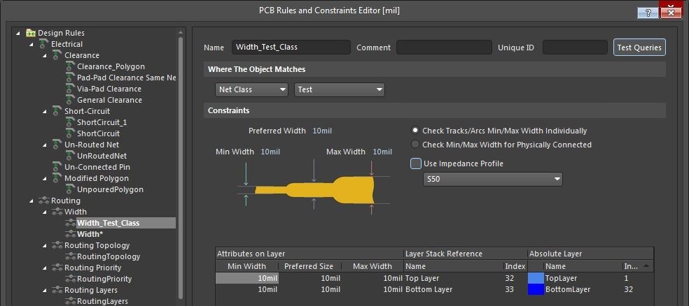
Once we’ve configured the name and object match of our new rule, we can then set up the width values. The impedance profile will always enforce a specific trace width when enabled. Altium Designer allows you to set up minimum, preferred, and maximum constraint values for your trace width rule and copper necessities (like copper thickness). You can also set up different width values for specific layers of the design. In our case you can see in the picture below that all the values have been set to 10 mils so no matter what we will only get a 10 mil trace width when routing nets in the “Test” net class.

Changing the routing width constraint values in the new rule
Creating a Rule for Minimum PCB Trace Spacing
Now that the routing width rule has been set, it’s time to set the clearance rule for the spacing. In the picture below you can see the PCB Rules and Constraints Editor again. On the left side you can see all the different rules and at the top of the list are the clearances. Using the same procedure as before, we have created a new clearance rule and named it “Clearance_Test”.
Changing the values of the clearance constraints in Altium Designer
Once again we have set up our new net class “Test” as the object match, but in a clearance rule you have two object matches in order to check the clearances between both. In this case we left the second object match set to “All”. The result of this is that Altium Designer will apply this clearance rule when checking between the traces of the net class “Test” and all other nets on the board.
In the constraints section you have a lot of different values that you can set. One thing that will help you here is that you can set the “Minimum Clearance” spacing value that we’ve marked in red, and that number will then be used to populate all the fields below. Once you’ve done that, then you can go through and make individual changes as you can see that we’ve done. If you want to change an entire line, as we did with the “Hole” values, click on that row’s name (“Hole”) and then enter your value. Once you hit “Return”, all the fields in that row will be populated with the same value.
Finally, you will want to set up your board layout session to prioritize these rules. Altium Designer gives you some choices in the “Preferences > PCB Editor > Interactive Routing” menu. As you can see in the picture below, you can choose between minimum, preferred, and maximum trace width rules.
Setting up interactive routing width source priorities in the preferences menu
At this point, you're ready to start routing! The interactive routing tools will interface directly with the design rules to ensure your trace width and spacing do not violate the rules you created. In addition, the routing you create will follow other important design rules, such as maintaining spacing to a reference plane for return path planning and maintaining clearances to other objects in the PCB layout.
If you're working on a high speed design or high frequency design, then crosstalk has the potential to create signaling problems. To verify whether the minimum trace spacing you've selected is the best option for your board, you can use a post-layout simulation to determine crosstalk between traces in your PCB. If crosstalk in your PCB is too intense, there are some simple changes you can make to your board to ensure crosstalk is within acceptable limits.
If you're tired of manually checking minimum trace spacing and width requirements, Altium Designer has the interactive tools you need. You can stay at your most productive and rest assured your traces are routed with your required width and spacing. You'll also have access to a complete suite of simulation features, high speed design tools, and manufacturing utilities in a single program.
Would you like to find out more about how Altium Designer can help you be more productive in your next PCB design? Sign up for a free trial or talk to an expert at Altium Designer.