The Best PCB Design Software Features A PCB Trace Impedance Calculator
PCB trace, pad, and via features are some of the most important in your circuit board and need to be carefully designed. The right cross-sectional PCB trace area and distance to the nearest reference plane will ensure your PCB trace impedance is consistent throughout your board. It can also help suppress temperature rise if your board will operate at a high current.
Choosing the right trace dimensions in your printed circuit board represents a tradeoff between these performance aspects. A top-notch printed circuit design program can help you choose the right PCB trace dimensions so that your PCB trace impedance is consistent throughout your board and your traces are routable. Altium Designer contains the interconnect design and routing tools you need for any PCB in a single platform.
ALTIUM DESIGNER
A powerful PCB design application that includes PCB trace impedance and width calculators for accurate routing and signal integrity.
There is a saying among the high-speed design community: there are those who have signal integrity problems, and those who will soon have signal integrity problems. Once the IC world blazed past TTL was introduced, switching between logic states became fast enough that everyone needed to take steps to ensure signal integrity in their traces. Impedance mismatch between traces used to be tolerable as only longer traces acted as transmission lines and those that did act as transmission lines could be easily terminated with a resistor and/or capacitor.
Nowadays, as components include higher pin counts, are routed through multiple layers in the stackup, and trace density has increased, ensuring your traces have a defined impedance is critical to ensuring your signals remain clean and transmission line effects can be avoided. Using the right multi-layer stackup and maintaining the right trace geometry is critical to maintaining signal integrity throughout your device.
Working with the right PCB design software will help ensure that you can maintain signal integrity throughout your PCB without manually defining the geometry of every single trace in your device. Altium Designer includes a PCB trace impedance calculator, PCB trace width calculator under IPC 2152, and a plethora of other important design tools. These important design features are incorporated into your design rules, making impedance controlled routing quick and easy.

A 3D view of a complex impedance controlled PCB in Altium Designer.
How to Enforce Controlled Impedance Routing
Obviously, the relationship between ground plane placement, layer stackup, and trace geometry in your circuit board are interrelated. Changing the stackup and copper ground plane location will change the trace geometry required to maintain the right impedance value during routing. This will also affect the power dissipated along a trace, which then affects temperature rise. Trace impedance is also related to the dielectric constant of the substrate material and is also affected by temperature.
When it comes to calculating copper microstrip trace width and thickness for a given impedance value, you will need to solve a transcendental equation for the ratio of trace width to thickness, where the height of the trace above its ground plane is used as a parameter. This requires manually calculating an intersection between the microstrip trace impedance curve and a linear function defining the width to thickness ratio. The right design software can implement this calculation for you, saving you time to spend designing your board instead of calculating this important parameter.
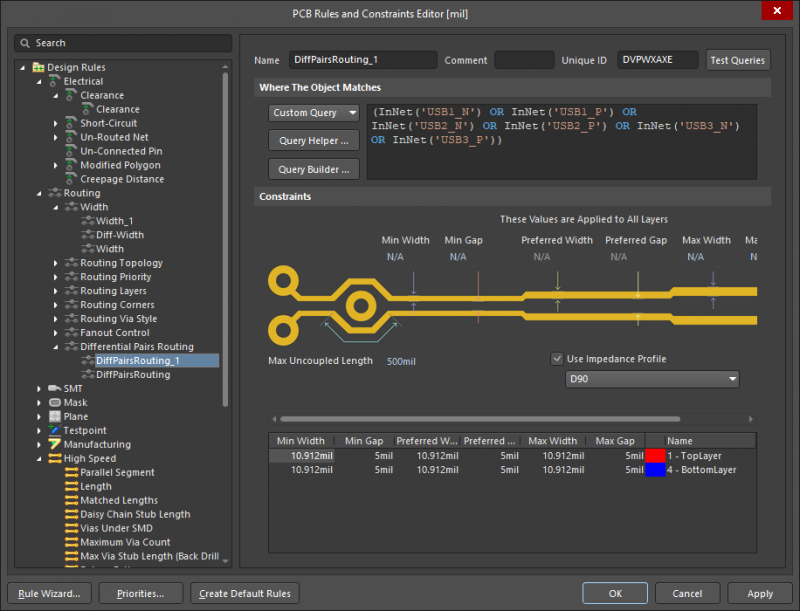
Many signal integrity problems can be alleviated with differential pair routing as these traces can reject common mode noise in a printed circuit. They also don’t require the use of a ground plane as a return signal is routed alongside the primary signal. This also helps maintain characteristic impedance as long as you maintain proper clearance and consistent trace length. These constraints can also be defined within your design rules with the right design software.
Ensure Impedance Control with a PCB Trace Impedance Calculator
Once you’ve determined the right trace geometry you need for your board, you’ll need to route your traces throughout your board. The goal is to ensure signal integrity while making the required connections. It is generally a good idea to minimize the use of vias on interconnects in your printed circuits as they can act as impedance discontinuities and can couple noise from nearby ground or power planes into your signals.
Managing characteristic impedance and differential impedance can be difficult. The right routing tools in your PCB design software can save you a significant amount of time and help you easily implement the right routing strategy. Your routing features should interface with your design rules and constraints as this allows you to define the appropriate trace width tolerances and clearance requirements between neighboring traces. The goal is to keep crosstalk and other signal integrity problems to a minimum while enforcing impedance control in your PCB layout.
- Working with trace impedance calculators can be confusing, but the right design software can help you ensure your trace impedance is accurate and complies with important design standards.
Learn more about trace impedance calculators and formulas in your design software.
- Most PCB design packages include a number of autorouter options. Choosing the right can expedite your PCB layout process and ensure you comply with your design rules.
Learn more about autorouting algorithms in your PCB design software.
- With differential or single-ended routing, you’ll need to define net clearance rules and ensure length matching throughout your traces. Learn more about working with net clearance rules in your PCB design software.

Altium Designer’s differential impedance rule manager window.
Using an IPC 2152 Calculator for PCB Trace Widths
Determining the appropriate trace width for a particular temperature limit, current density, substrate material, and layer count is not an easy problem. Fortunately, the IPC-2152 standard includes appropriate PCB trace sizes for these different situations. You can easily calculate your trace widths from standards, or you can exploit internal design rules in your PCB software.
Once you determine the appropriate trace size for your circuit board as a function of current density, you need to enforce that size during printed circuit design and layout. You’ll need PCB design software that enforces integration between your routing tools and design rules. This allows you to place multiple traces with the required cross-section automatically, rather than manually defining every trace on the board. You’ll be more productive and more accurate within your PCB design flow.
Altium Designer’s IPC 2152 Calculator Does the Work for You
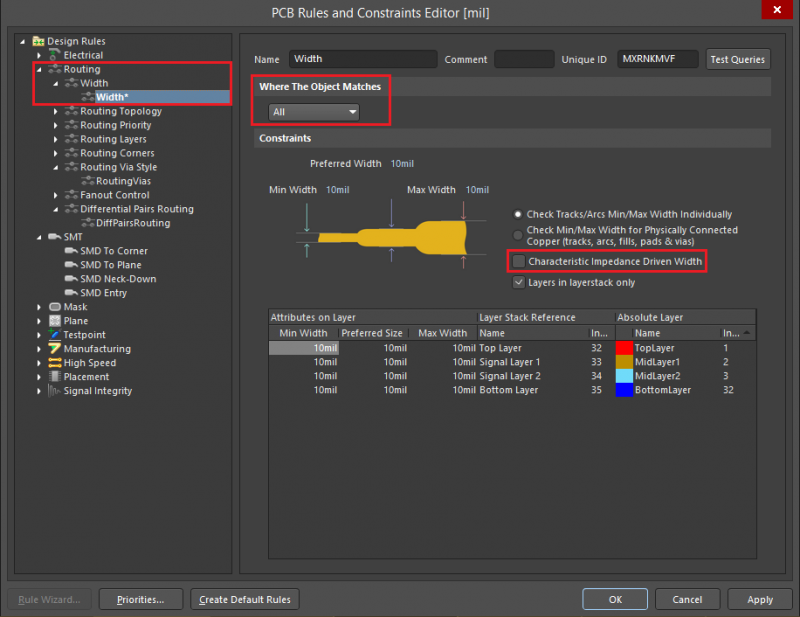
Once you’ve entered the board materials and their trace thicknesses into the layer stack manager, the impedance calculator will take the industry standard formulas for calculating stripline and microstrip routing widths and plug those numbers into the design rules for you. Other considerations like relative permittivity or the dielectric constant are not taken into account in this process. Once you input your desired impedance values into your impedance profiles, the design rules will automatically update with the correct routing widths and you are ready to route.
- The rules and IPC-2152 industry standards for printed circuit trace widths can be determined from a standard nomograph.
- Defining the required trace dimensions in your PCB design software as design rules saves you time when routing and verifying your circuit board. Your design software should enable quick trace routing by interfacing directly with your design rules.
- The rules-driven design engine in Altium Designer interfaces with an automated field solver for impedance control and an IPC-2152 trace width calculator for thermal control.

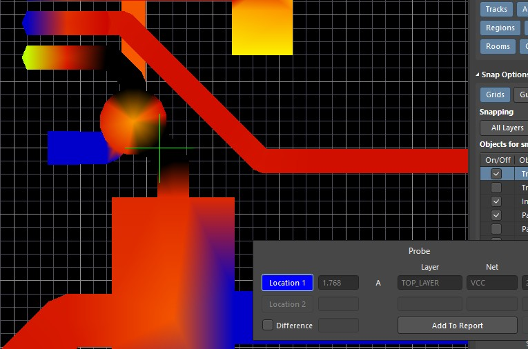
You can use the PDN Analyzer in Altium Designer to identify hot traces and vias.
Ultra-Accurate PCB Trace Impedance Control and Thermal Control
Third party impedance calculators that you might find on the internet can help you get an idea of the best trace geometry, arrangement, and layer stack that help you control impedance in your board. However, these calculators will never interface directly with your PCB layout software as part of your design rules. You’ll still be stuck checking the impedance of every trace on your board, even if you use automated or interactive routing.
While you can’t change the laws of physics or modify the real equations that define impedance of your traces and vias, the right design software lets you control how your board is routed based on desired impedance values. When your software is built on the back of a single rules-driven design engine, trace impedance calculations can be included as an integral part of your routing tools, ensuring your trace impedance will always take a desired value.
Your design rules are meant for more than just checking routing parameters, component placement, and connections between components. They make it easy to verify your design as you create your circuit board layout, and you can immediately see if your design needs to be changed. This all relies on working in printed circuit design software that unifies your design rules engine with your layout and routing tools, and this is exactly what you’ll find in Altium Designer.

Defining PCB trace impedance as a design rule in Altium Designer
Altium Designer Makes PCB Trace Width Calculations Easy
PCB design used to involve an army of engineers to develop a circuit board, and each member of the design team would be responsible for different aspects of the project. Usually, there was someone who would handle the board layer stack configurations and calculate trace widths and spacing for controlled impedance routing. The right design tools cut down the time required to design PCB trace widths for controlled impedance and minimum temperature rise under IPC-2152.
Altium Designer packs the power of a circuit board design army into a single, powerful application with all the tools you need. You’ll have a complete set of design tools for building schematics and layouts, followed by preparing for PCB manufacturing and PCB assembly processes. All the design tools you need, including an integrated field solver for PCB trace impedance calculations, will interface directly with your design rules as you create your board. The days of using multiple programs for a single design are over.
- If you want to create an ultra-accurate circuit board for high-speed components, you’ll need to work in an environment that unifies your layout features and rules-driven design engine.
Learn more about the unified design environment in Altium Designer.
- When it comes to calculating your trace widths and spacing for controlled PCB trace impedance routing, Altium Designer has the solution you need. With its enhanced layer stack manager, Altium Designer supplies you with a library of board materials to build your circuit board layer stackup.
Learn more about designing the right stackup in Altium Designer.
- Fusion between autorouting and interactive routing is a powerful tool in controlled impedance design and circuit board layout. Integrating these features into a single tool saves you time and ensures routing accuracy.
Learn more about auto-interactive routing in Altium Designer.
There’s a lot on your shoulders as a PCB designer. Let Altium Designer lift some of that load off of you with its embedded trace impedance calculator to configure your design for controlled impedance routing. These important design features are integrated into a single program on top of a rules-driven design engine. This engine ensures that your PCB trace widths will comply with important design rules that govern routing standards and manufacturability and PCB assembly.
You’ll also be able to prepare deliverables for PCB manufacturing without sending your data to an external program. This saves you the time of finding your own calculator and running the numbers yourself. Try the most comprehensive set of PCB design utilities that are built around industry standards: it’s time to switch to Altium Designer.
Altium Designer on Altium 365 delivers an unprecedented amount of integration to the electronics industry until now relegated to the world of software development, allowing designers to work from home and reach unprecedented levels of efficiency.
We have only scratched the surface of what is possible to do with Altium Designer on Altium 365. You can check the product page for a more in-depth feature description or one of the On-Demand Webinars.
