RF PCB Material Comparison for mmWave Devices

When some designers start talking materials, they probably default to FR4 laminates. The reality is there are many FR4 materials, each with relatively similar structure and a range of material property values. Designs on FR4 are quite different from those encountered at the low GHz range and mmWave frequencies. So what exactly changes at high frequencies, and what makes these materials different?
To see just what makes a specific laminate useful as an RF PCB material, take a look at our guide below. We’ll show you some examples from popular vendors and how you can use these in your PCB stackup.
When Do You Need an RF PCB Material?
This is a fair question and it relates to some important tasks in systems analysis. There are a few different considerations a designer should examine when qualifying an alternative PCB substrate material should be used. Here’s a short list of some dimensions you might look at when selecting an RF PCB substrate material.
- Loss tangent: This is the first major area that PCB designers will use to start comparing material options.
- Dielectric constant: Although this is sometimes misunderstood, and everyone tends to just go for low-Dk laminates, but high-Dk laminates can also have low loss tangent and other benefits.
- Thermal properties: There are multiple thermal properties, but the most important are probably glass transition temperature and CTE.
- Workability in fabrication: Designers leave this up to their fabricator at their own peril. It’s best to contact your fabricator regarding availability of materials, their ability to work the board, and availability of materials.
- Thickness: You can’t just choose any thickness you want, you’ll need to check with your fabricator on their preferred stackup. If you know which layer thicknesses they can support, you can usually get your design close enough to the fabricator’s specifications.
- Dispersion: I’ve put this at the bottom of the list as it tends to matter least for mmWave applications. The bandwidths in mmWave devices may be small enough that dispersion is negligible, but you should still check on this where possible.
Unfortunately, as is the case in many engineering problems, there is no perfect answer or perfect material that can perform in all these areas simultaneously. However, for high-reliability RF products, there are some common RF PCB substrate materials that are designed to support specific frequency bands without compromising on important thermal properties.
Well-known PTFE RF PCB Materials Vendors
Today’s standard materials for RF and mmWave devices are PTFE-based materials. Rogers is probably the best-known manufacturer of PTFE-based RF PCB materials, and the company manufactures a variety of high frequency PCB laminate materials. Some of these are specialized for use in the Ka and W bands (car radar and future 5G bands). If you’ve ever downloaded a PCB reference design for an RF product, their example layout was probably built using Rogers.
Another well-known vendor is Isola, whose RF PCB materials options target a range of frequencies up to the W band. In addition to some RF PCB materials, they also offer a range of standard FR4-grade laminates. One laminate I tend to default to is 370HR, and I’ve used this to build several networking products and custom IoT platforms. It works perfectly well at Wifi frequencies for RF PCB layout and routing, and it will work well for most digital applications.
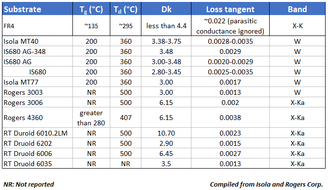
Some examples of PTFE RF PCB materials and the performance of each is shown in the table below. Note that some typical values for low-Tg FR4 are included in the X-K bands as a baseline.

We can’t show every possible substrate option for RF PCB design, but I’ve focused on these as they are popular options for a few reasons. The loss tangent values are what you’d expect compared to typical FR4 materials (about a factor 10 lower), and these materials have high decomposition temperatures compared to typical FR4 laminates. These are some of the main characteristics identified in IPC slash sheets, and your fabricator may suggest an alternative PCB material that will be compatible with your desired laminate.
Whether you want to use one of the options in the above table or some other material platform, be mindful when reading datasheets. The material vendor should be able to verify the values they quote within the listed operating conditions. You can learn much more about dielectric materials for your substrate and test methods from John Coonrod of Rogers Corp.
Working With PTFE and Other Materials
Every design decision comes with tradeoffs, and PTFE-based materials have some basic disadvantages compared to FR4:
- High CTE, so thermal expansion puts more stress on copper elements
- PTFE does not easily bond to other materials, thus a bondply is used
- PTFE is a soft substance can it can be easily distorted
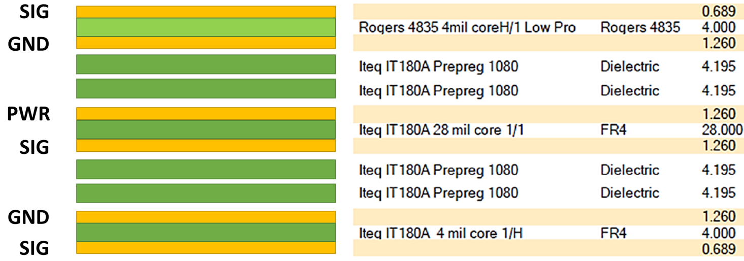
Then there is the cost. PTFE laminates are a specialty material despite their popularity, so RF devices are not normally built with PTFE throughout the layer stack. One option is to use a hybrid stackup, where the PTFE laminate is placed on the surface layer and high-frequency signals are only routed on the PTFE laminate above a plane layer. An example stackup table for a 6-layer RF board is shown below.

Watch for New Innovative Materials
Materials companies will continue to develop innovative low-loss, low-dispersion solutions. Some of the newest experimental materials are targeting fiber weave effects and will attempt to solve these with smoother materials. With the right PCB layer stackup tools, you won’t be restricted to specific materials values, you can enter custom materials data from your manufacturer into your stackup design.
Once you’ve selected an appropriate RF PCB material to support high frequency layout and routing, you can create a high quality stackup with Altium Designer®. All Altium Designer users can use the EDB Exporter extension to import their design into Ansys field solvers for advanced signal integrity simulations.
When you’ve finished your design, and you want to release files to your manufacturer, the Altium 365™ platform makes it easy to collaborate and share your projects. We have only scratched the surface of what is possible to do with Altium Designer on Altium 365. You can check the product page for a more in-depth feature description or one of the On-Demand Webinars.
