PDS Impedance: The Traditional Approach To PDS Design vs. Energy Flow

As noted in previous blogs, one of the challenges that we face on an on-going basis is thinking that we have killed all the mythological creatures that result from trying to make certain design elements subject to “black magic” rules-of-thumb versus traditional, readily-provable design methodologies. Just when we think we have finally slain one of these creatures, it raises its ugly head again. Probably the one aspect of design where this occurs most frequently relates to power delivery network (PDN) or power distribution system (PDS) design. This is because getting a PDS design correct can be one of the most difficult design tasks in overall product development. At Speeding Edge, we believe it is incumbent upon us to debunk information that, at best, is misleading or, at worse, will cause a design to fail.
PDS Design: Reviewing What is Important
Recent questions posed to us focused on the traditional PDS impedance design approach, versus the “energy flow” view of design. Here are the salient aspects of the questions and our response to them. The assumptions are shown in italic type, and our responses are shown in regular type. Those responses that appear in quotes are direct statements given by Lee Ritchey, Founder and President of Speeding Edge.
- The steady-state PDS impedance plays a significant role in PDS design.
- “There is no such thing as a steady-state in the PDS. The assumption being made is that things are static. This assumption flies in the face of what is the purpose of a PDS and how it operates. By definition, circuits attached to the PDS are active and not in the ‘steady-state’.”
- A target impedance is chosen so that the voltage ripple margin budget is satisfied across the frequency range of interest.
- “This is correct. When you design the PDS, you are trying to minimize ripple. Ripple is the result of extracting charge from the PDS, which is a reservoir of charge. The ripple you get depends on the frequency where you are trying to get the charge, and how low the PDS impedance is at that frequency. The whole world pretty much understands how the PDS works.”
Taking the foregoing one step further, in one of my previous articles, I described the elements that factor into the PDS design process to determine PDS impedance. For the sake of convenience, they are repeated here.
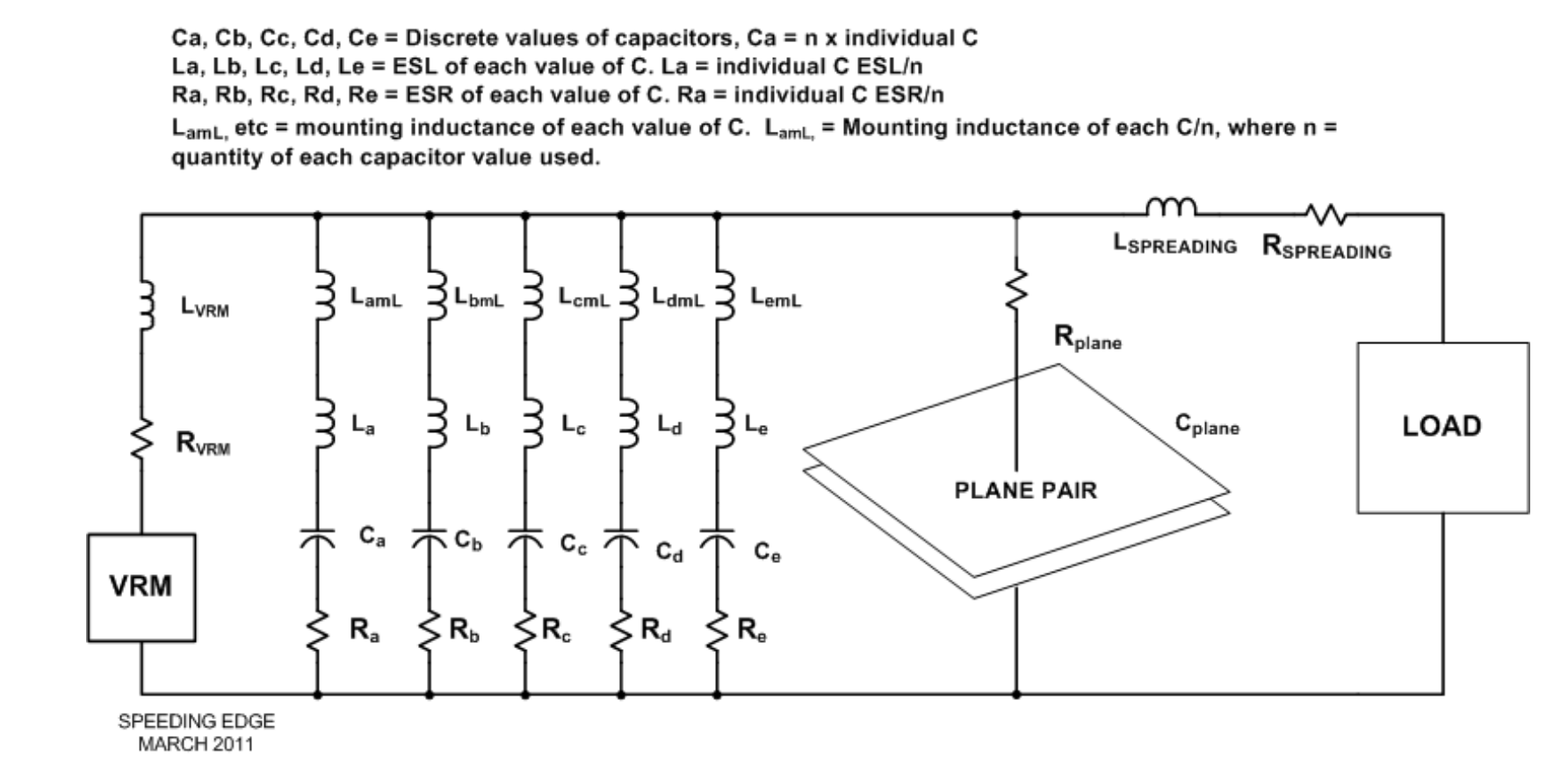
Figure 1 shows the PDS impedance of typical design with all of the elements that comprise a PDS.
These include:
- Voltage regulator module (VRM) also referred to as point of load (POL). This is the module that creates the DC voltage.
- The capacitors that are mounted on the board.
- Capacitance provided by neighboring plane layers.

Each of these elements has a limited range of frequencies wherein they are effective as follows:
- VRM: The VRM is capable of maintaining a stable DC voltage with noise concentrated from a few kHz up to the edge frequency for the PWM signal. Note that you could opt for a higher switching frequency with the right PWM driver to reduce conduction losses during switching.
- Capacitors: The use of capacitors is intended to provide low PDS impedance from a few kHz up to about 100 MHz.
- Plane Pair: The plane capacitor is capable of supplying charge when the current burst waveform’s bandwidth spans above 100 MHz. Note: The source of all EMI problems that we have troubleshot over the past few years has been the lack of any large plane pair capacitance in the board. As an aside, it’s important to note that, when boards get small, there is no plane capacitance. In these instances, the capacitance must be within the IC component itself.
These elements are placed in parallel and can produce a complicated resonance spectrum that spans across the ripple waveform’s bandwidth. The job of the PDS design engineer is to manage the foregoing elements such that a low impedance is maintained across the bandwidth at which the loads operate.
- A flat PDS impedance will, by definition, have no resonances and will ensure transient noise is minimized
- “A flat impedance is not necessary. A low impedance at the frequencies where you are operating is. The impedance does not need to be flat across all frequencies if the loads don’t operate at some frequencies. (An RF circuit is an example of operating over a very narrow range of frequencies).”
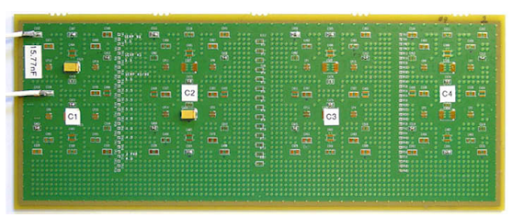
- The location of the decaps doesn’t matter much if the power-ground planes are very close (due to a low power-ground cavity spreading inductance compared to the mounting inductance of decaps). This is shown in your book by comparing two near-identical impedance plots with decaps, one very near and one very far from the load.
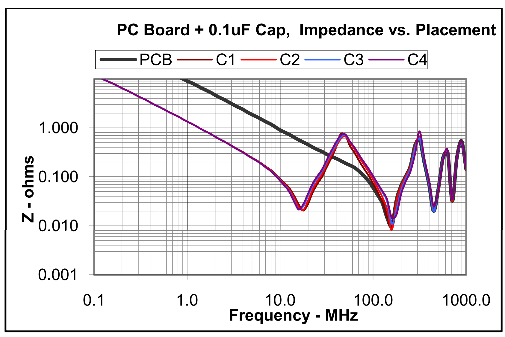
- “The statement about the location of the decaps is true. The use of the term ‘power-ground cavity’ does not make sense. It is plane capacitance. The charge is going to be extracted from it like every other capacitor. The reason for a plane capacitor—most all of the frequencies that are involved in modern logic are higher than what discrete capacitors can supply because of their inductance. Figures 2 and 3 from our book support this.”


- Ferrite beads introduce excess inductance that would require us to use a large amount of capacitance to compensate for its effects and make the PDS impedance flat again.
- The necessity of maintaining a low PDS impedance across the entire frequency range of a given PCB negates the use of ferrite beads. This is because ferrite beads in the power path destroy the impedance of the PDS. After all, by definition, ferrite beads have high impedance. The energy flow view, in contrast to the traditional PDS impedance design approach, is held by some “industry experts” who focus on the behavior of the electromagnetic field instead of voltage and currents for board design. The claims and refuting of them are detailed below and follow the same format as above. The assumptions are shown in italic type, and our responses are shown in regular type. Those responses that appear in quotes are direct statements taken from Lee Ritchey.
- Voltages and currents are just consequences we see at the conductor boundaries due to the interaction between the electromagnetic field and the surrounding conductor. The EM waves that must deliver energy at a particular instance will never fit within the above “steady-state” picture. Moreover, logic signals are step functions and step waves.
- “The difficulty with this whole topic is that there are these so-called energy fields, and they somehow factor into the PDS design process. I have a difficult time even addressing these claims because someone is imagining a problem. They don’t have proof that it exists, but they are going to solve it anyway. Out the gate, they make some basic statements that are patently false. For instance, logic functions are square waves, not just step functions.”
- When the first transistor at the load switches and demands energy, some of the energy is delivered through the energy stored in the transmission lines (behind the switch and connected to the related power-ground rails) by EM fields. Then a depletion wave (a reflected negative voltage edge) has to travel through the die, package, and through the space between the power ground via pairs attached to the BGA up to the cavity. Then the depletion wave travels through the power-ground cavity (in a concentric circular fashion) and up to the decoupling capacitor through the space formed by via pairs connecting to the decaps.
- “First, there is no such thing as a depletion wave. It does not exist. The key thing to remember about the above statement is this: A theorem is assumed to be false until it is proven to be true. All of the information about EM fields cited above is a theory because there is no evidence that it is valid. The burden does not rest with us to prove the proponents of this theory wrong. I want proof showing that what they say is valid. This holds true for the preceding as well as for the rest of the claims made by the people touting the EM flow view as represented below.”
The [depletion] wave enters the capacitor structure, moves very slowly inside the capacitor (due to a very high Dk) and reflects at the open end. This reflecting wave extracts and passes a little bit of energy at the terminals of the capacitor. This energy is carried by a reflected wave back to the load switch, delivers the energy, and does the same process again and again. The energy is being sucked by the load instead of energy sources pushing the energy to the load!
The Energy Flow View
- Very few people have written on how energy is actually extracted from the power-ground cavity through the space between power-ground via pairs. The power-ground via pair impedance at the point of contact on the plane pair is around 50 ohms. The impedance then decreases radially outwards in the cavity. This means there'll be multiple reflections back and forth (in concentric circles) as the energy is sucked up from the cavity by the waves. These concentric back and forth reflections grow radially outward till they reach the decoupling capacitor. It takes time for all this to occur.
- There is very little capacitance in the planar cavity. Capacitance benefit is negligible. Closely spaced power-ground planes lower the cavity impedance. The lower the impedance of the cavity, the more energy that can be carried by the depletion wave per cycle (1 round trip time—from load to the decap and back to the load).
- The amount of energy that can be extracted by the waves can be increased by reducing the entry point impedance (space) at the capacitor connection. This means the smallest capacitor package size is the best.
- A decoupling capacitor is a two-port open-ended stub. It takes time to extract energy from it. The depletion wave after entering the capacitor moves very slowly through it (due to very high Dk) and reaches the open end. It then reflects back. When it reaches the entry point, some of the energy is carried by the depletion waves back to the load.
- The closer the capacitor is to the load, the shorter the round trip time needed for a depletion wave to go from the load transistor to the capacitor (energy storage); extract energy from the capacitor, and take it back to the load. From the above points, it is clearly evident that the best location for the placement of a decoupling capacitor is directly across the power-ground balls. This can be easily attained by using a 1uF 0201 size capacitor and via-in-pad technology.
This view tells that, even though the steady-state view of the PDS impedance may be near identical when a decap is close or far (for closely-spaced power-ground planes), the load can suck the energy through EM waves—A LOT faster if the decaps are placed right at the power-ground balls. Hence the placement of the decap is critical even if power ground planes are very close to each other. I’m torn about these two radically different perspectives of looking at PDS design. I’ll be delighted to hear your thoughts in this field perspective view. Both views provide contradicting design philosophies. We need to choose one!
Ritchey concludes by saying, “This kind of hand-waving does a real disservice to those engineers who are designing products based on long-proven technologies and design methodologies. The proponents of the EM flow view are making a huge number of claims, none of which have been shown to be valid. As a result, no one should implement their design approach until the proponents can show that what they are claiming has validity. In contrast, there are books and books of proof that the traditional PDS design approach is a valid one. This is a clear example of ‘if it ain’t broke, don’t fix it.’”
Summary
It can be very difficult to ascertain the correctness of a proposed design methodology, especially one which is touted as coming from industry experts. Our approach to these untried methodologies is to be shown validation of the claims with real, measurable data. When that data does not exist, we advocate adherence to tried-and-true design methodologies, as there is plenty of data to support them, and plenty of working hardware that has been successfully implemented time and again.
Would you like to find out more about how Altium can help you with your next PCB design? Talk to an expert at Altium, or continue reading about analyzing PI-DC with Altium’s PDN Analyzer.
References:
- Ritchey, Lee W. and Zasio, John J., “Right The First Time, A Practical Handbook on High-Speed PCB and System Design, Volumes 1 and 2.”