Power Delivery Analysis: Getting Started with PDN Analyzer
If you’ve ever been involved in RF design, high-speed design, high current design, or all these areas combined, you know the importance of power integrity in your PCB. If power delivery in your next PCB design is a critical performance factor, you need simulation and analysis tools that are accessible alongside your standard PCB design features. Here’s how the PDN Analyzer feature in Altium Designer can help you diagnose and correct your power delivery issues and build advanced electronics.
ALTIUM DESIGNER
A unified PCB design software package that contains all the design and PDN analysis tools you need to build advanced electronics.
Power integrity and signal integrity are some of the most important aspects in many PCBs. Maintaining stable voltages and suppressing noise ensures your PCB will operate as designed. If you want to maximize your productivity, you need a software package that integrates your power integrity simulator into your PCB design software.
The right PDN should take data directly from your PCB layout, and it should show you the voltage and current density distribution in your PDN. Voltages and current density on the power and ground nets are functions of all PDNs in your PCB, and these quantities are unidentifiable when each PDN is examined in isolation. PDN Analyzer’s unique voltage regulator models (VRMs) enable these interactions to be captured while simplifying setup and increasing simulation speed.
Whether you are a seasoned power integrity expert or a beginner, gaining insight into your design’s voltage and current density distribution, current direction, and hot spots is simple and intuitive. With PDN Analyzer, results are displayed in a replica of your PCB layout, which is generated using your layout data in Altium Designer’s PCB Editor. You’ll be able to see power nets alone, or as a rendered overlay against the complete PCB in 2D or 3D. Take a look at our guide to getting started with PDN Analyzer and how you can visualize your voltage and current density distribution in your PCB.

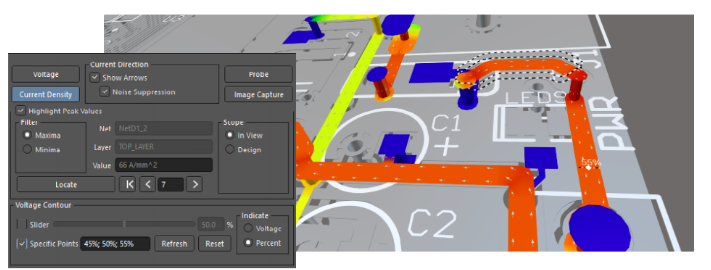
3D visualization of current density in a PCB with the PDN Analyzer
Getting Started with PDN Analyzer
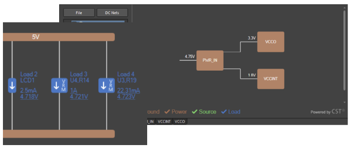
To get started with PDN analyzer, simply bring up the PDN Analyzer window and define the structure of your PDN. The image below shows how to set up a simultaneous multi-network simulation for examining the DC voltage and current density distribution in an entire PCB. The typical structure of a PDN is hierarchical; voltage and current density can be examined throughout each level in the network, or within individual power nets.

Setting up a multi-network PDN analysis by defining sources and loads in your PDN.
Any PDN analysis tool should help you determine how multiple PDNs interact with each other. By defining a hierarchical structure for the PDN in your PCB, you’ll have a clear view of how the current density and voltage are distributed throughout the power nets. The PDN analysis performed by this tool relies on solving Maxwell’s equations with a field solver, so it can consider complex geometries like vias, unique trace geometries, and polygons in your PCB layout.
Move Seamlessly Between PCB Design and Simulation
When your PCB design software creates a unified design environment, you can move between your design and simulation features with ease. Altium Designer gives you the tools to diagnose your power delivery problems early in the design process. You’ll be able to produce more powerful products with greater reliability.
- You can learn many important performance aspects of your PCB with PDN analysis. Learn more about the importance of DC PDN analysis.
- Power integrity in your system is difficult, but the right design practices and PDN analysis tools can help ensure your components won’t lose power during operation. Learn more about best design practices to ensure power integrity.
- PDN analysis is about more than calculating voltage drops, you can visualize where power is consumed in your PDN as your board is put under stressful conditions. See an example of how easy getting started with PDN Analyzer can be.
PDN Analysis With Advanced Visualization Tools
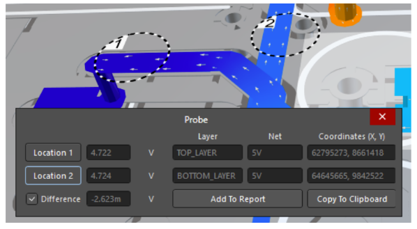
The PDN Analyzer tool can be used to interactively measure voltage, current density, or via current at any point in a PCB layout created in Altium Designer. Net, layer, and X,Y coordinates are updated in real time, along with the probe value to ensure that the correct point is “picked”. The pick points are marked graphically in 2D/3D and can be easily added to an HTML report.
Once you set up the hierarchical structure of your PDN and each branch with loads, the tool is ready to start calculating voltage and current density throughout the network. The PDN analyzer will model power sources as VRMs within the hierarchical structure. Once you switch to the 2D/3D view of your PCB, you’ll be able to see how voltage and current density vary throughout the power and ground nets in your board.

Voltage and current density probing location settings.
When viewing your power distribution in 2D or 3D, you can set probes in your PCB layout to see the voltage and current density at different points. This is a great way to inspect specific points in your PCB power and ground nets for excessive power drop or potential hot spots. You can identify and quickly correct these problems in the PCB editor.
Altium Designer Has the Advanced PDN Analysis Features You Need
Because Altium Designer integrates your entire set of design and simulation tools into a single program, you can quickly correct PDN problems in the PCB editor. The PDN Analyzer replicates your PCB layout and provides an easy way to pinpoint these problems with probes in the 2D or 3D visualization features. You can then quickly switch back to the standard layout and routing features in Altium Designer to improve your PCB layout.
- In more advanced products, like high-speed digital and high-frequency analog systems, a PDN needs to be carefully designed to prevent jitter and ensure consistent power delivery. Learn more about power system design for high-speed boards.
- PDN analysis requires mapping voltage and current density in a PDN with any geometry, including split planes.
Learn More about split planes in your PDN and why you should avoid them.
- Return paths in your board determine power delivery and signal integrity in high-performance electronics. Learn more about planning AC and DC return paths in your ground plane.

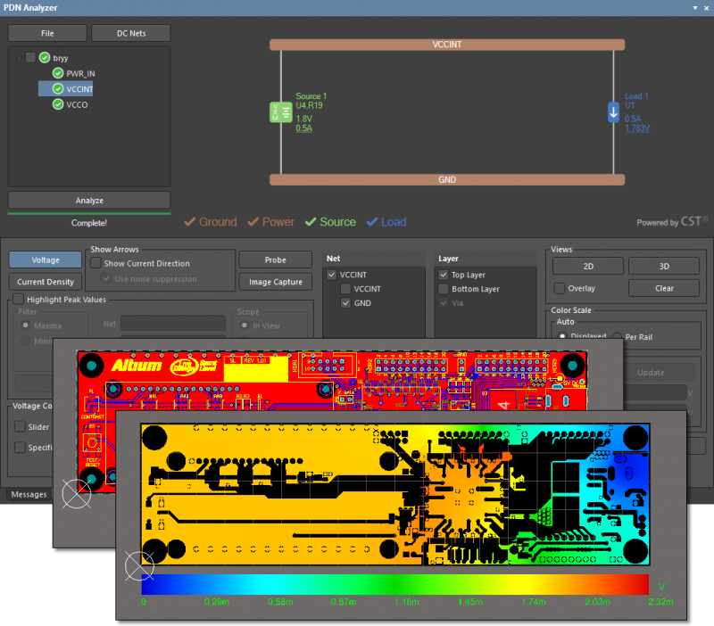
Multiple PDN analysis views for a complex PCB layout.
Get the Most Accurate Power Delivery Results with PDN Analyzer
PDN Analyzer (powered by CST®) shortens your design cycle by enabling all designers to easily identify and solve power delivery problems during the PCB design process. With a wide range of analysis capabilities, PDN Analyzer streamlines power delivery analysis. You’ll have a simulation tool to help you locate, understand, and resolve power delivery problems without relying on expensive prototypes, complicated tools, or dedicated power integrity engineers.
The PDN Analyzer utility is accessible directly from Altium Designer; there is no other program to download or install. This powerful tool follows the same trend as other utilities from Altium: it takes PCB layout data directly from the PCB editor and allows you to run power integrity simulations. The utility provides PDN analysis results visually as heat maps, allowing you to see voltage and current density distribution throughout your PDN.
Analyze Your PCB Design Using an Integrated PCB Design Platform
Since Altium Designer operates in a unified design environment, you’ll have everything you need to access layout, routing, and simulation tools from the PCB Editor window. Accurately mapping your power distribution is the cornerstone of PDN analysis, and you can easily access this functionality through the PDN Analyzer tool within the PCB Editor. You can quickly identify and correct power delivery problems in Altium Designer’s intuitive interface.
- Altium Designer runs on top of a rules-driven design engine, allowing you to keep your board error-free. You can define important industry standards and DFM requirements as design rules, which ensures your board will be manufacturable at scale. Learn more about rules-driven design in Altium Designer.
- All your layout data in Altium Designer’s PCB editor can be quickly imported into the PDN Analyzer tool for power delivery simulations. Learn more about using the PDN Analyzer in Altium Designer.
- Altium Designer includes many new layout and routing features that are accessible in the PCB editor. Learn more about the newest features in Altium Designer.
Altium Designer includes all the design, analysis, simulation, and component management tools you need to design world-class PCBs. If you’re just getting started with unified design, Altium will be there with the resources you need for success. You’ll have access to the Altium Academy, webinars and podcasts with industry experts, and the AltiumLive Forum. No other PCB design software company is this invested in your success.
The PDN Analyzer addon provides unsurpassed integration by running simulations directly from layout data in the PCB editor. If you’re tired of cobbling together multiple programs into a single workflow, it’s time to try a new design and simulation application: it’s time to try Altium Designer.
Altium Designer on Altium 365 delivers an unprecedented amount of integration to the electronics industry until now relegated to the world of software development, allowing designers to work from home and reach unprecedented levels of efficiency.
We have only scratched the surface of what is possible to do with Altium Designer on Altium 365. You can check the product page for a more in-depth feature description or one of the On-Demand Webinars.
