Advanced High Density PCB Design in Altium Designer
HDI PCB design and manufacturing pushes electronics and circuit boards to their limits. As electronics become faster and more capable, they require greater functionality in a smaller package. From smartphones to smartwatches and other IoT devices, HDI design is slowly becoming the norm rather than the exception. Keeping up with new technology and design techniques means that designers need to rethink how they layout components, as well as design interconnects and vias in their boards.
If you want to be successful with your next high-density PCB design project, you need the right design tools to help with routing and rules checking. Only Altium Designer integrates rules checking into your layout and routing tools, giving you a complete platform for advanced electronics design and much more.
ALTIUM DESIGNER®
The only unified PCB design package with a full suite of CAD tools for high-density PCB design, layout, and routing on multilayer HDI boards.
Modern electronics carry more components and functionality than ever before, and designers need to understand many of the finer points of high density interconnect (HDI) PCB design. It starts from a simple idea: reduce the size of traces, vias, component, and pads in order to fit more components into a smaller area. However, this requires changing the manufacturing process, and any HDI PCB needs to be manufacturable at scale. Here’s what goes into successful high-density PCB design and routing:
- HDI PCB Stackup Design
- Defining Microvia structures
- BGA Breakout in HDI Boards
Altium Designer gives you everything you need for success in these areas and much more. Here’s how you can be successful when designing your next HDI PCB and how you can prepare for circuit board manufacturing with HDI PCB processes.
HDI PCB Stackup Design
Implementing HDI design techniques on your board requires designing the right stackup. You’ll need to ensure that you can route the high density of signals you need between components while providing EMI shielding and ensuring signal integrity. Accessing the inner signal layers requires designing the right vias and designing landing pads that link directly to your traces. Your PCB stackup forms the foundation of your HDI boards, and working with the right stackup will make your routing and layout tasks much simpler.
Creating an HDI PCB Stackup
An HDI PCB stackup does not require a specific number of layers. Any circuit board with 8 to 32 layers or more could be considered an HDI board when the trace widths are small enough. Altium Designer gives you access to a powerful set of via design tools for working with multilayer HDI boards and a layer stack manager to create your new circuit board substrate. The right layer stack manager allows you to place as many layers as you like in your HDI circuit board and define via transitions between each layer.
- Routing between the inner layers of your HDI PCB takes creative use of vias. You can save a significant amount of space with blind and buried vias. Learn about working with blind and buried vias in HDI PCBs.
- Multilayer boards are a mainstay in high-density PCB design, and you’ll need to choose the right HDI stackup for your particular application. Learn more about designing your stackup for HDI PCBs.
- Designing vias for HDI PCBs is easier than you think when you use the right PCB design software. See how you can design blind and buried vias in Altium Designer.
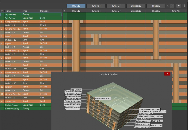
Controlled impedance routing in HDI boards requires an accurate impedance calculator in your layer stack manager.
Defining Microvia Structures
HDI boards require the use of microvias for layer transitions. Microvias are simply small vias that require a specialty manufacturing process (i.e., other than mechanical drilling). These structures are defined by the IPC-2226 HDI Design Standard. The various microvia structures you can access in Altium Designer are shown below, which includes staggered, skip, and buried types of microvias.
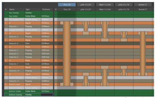
HDI PCB via definition in Altium Designer’s layer stack manager.
Staggered Blind Vias
Staggered microvias on a single side or both sides with buried through-hole vias between inner layers is the most common and lowest cost HDI PCB layer stackup. When using multiple microvias to connect inner layers, it is preferred the microvias be offset by some angle and the vias not be stacked (e.g., as in a crankshaft). This will minimize any thermal excursions if the vias heat up to high temperatures. Be sure to contact your circuit board fabricator for material and process compatibility if you plan to produce an HDI PCB at high volume.
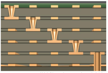
Build-up of multiple HDI PCB layers connected with buried vias.
Skip Blind Vias
A skip microvia is special in that it is used to ‘skip’ the next adjacent layer, as seen in Figure 7. Because a skip microvia can be the deepest of microvias, it is important that the designer be aware of a fabricator’s capability to produce and metallize such a microvia. Many circuit board manufacturers will not have this capability and will give your board no-bid status if they spot this in your Gerber files. With all blind vias, the aspect ratio may be reduced to 0.7:1 or even 0.65:1, so that the surface pad and target pad will be larger than the via length. The via is quite susceptible to fracture at its neck when light copper foil is used to place these vias.
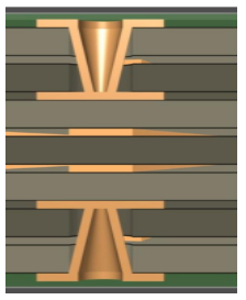
A skip microvia can be used to skip a layer in a multilayer circuit board.
Stacked vias
Stacked microvias use the least amount of board real-estate but are significantly more difficult to fabricate. This stems from the need for the target land of the top microvia having a solid metal surface to connect to. The process requires filling of the microvia either with conductive materials and plating it over (VIPPO) or with the use of “super-fill copper plating” capable of solid copper plating the microvia interior (see the image below).
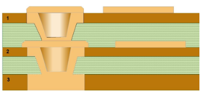
Stacked microvias require a solid metal surface for the ‘landing pad’ on top of the microvia. The lower portion of the microvia is produced with a laser, and the void is filled and plated over.
Currently, it is recommended that stacked microvias not be stacked on top of a mechanically-drilled buried via. Reliability concerns have arisen from this practice. Be sure to contact your PCB fabricator about this construction and read the IPC White Paper on Performance-Based Printed Board OEM Acceptance-Via Chain Continuity Reflow Test: The Hidden Reliability Threat-IPC-WP-023 (May 2018).
Mechanically Drilled Blind/Buried Microvias
Microvias can also be mechanically drilled, although these usually have larger diameters (>6 mil) than laser drilled microvias and have low aspect ratio. The cost per via is also higher than the cost per laser drilled via as these thin drill bits fracture often and need to be replaced frequently.
BGA Breakout in HDI Boards
Fine-pitch BGA fanouts are routed either using microvia-in-pad or by using a microvia that is only touching the SMT pad. Note that, for 0.5 and 0.4 mm pitches, the via holes are not in the center of the lands. This is to increase spacing between traces on the inner layers beyond a minimum of 0.075 mm. When selecting design rules for fine-pitch BGAs, be sure to contact your PCB fabricator to determine which geometries and tolerances they can support.
In addition to the traditional N-S-E-W dogbone breakout of BGAs, microvias facilitate two new BGA breakout methods that greatly increase routing density and lower layer counts. This is thanks to the much smaller size of microvias. These two methods are channels and swing-via placement.
Channels
When a BGA’s total number of signal escapes begin to exceed 400 pins, microvias should generally be used for breakout as rows that cross the BGA, rather than on the peripheral. These form ‘channels’ on the inner-layers and far side of the circuit board. These channels allow access to internal signals in the BGA, thus fewer layers are required for total breakout.
The BGA in Figure 11 is an 1153 pin (34x34) BGA (1.0 mm pitch) and with 132 possible routes per layer (1 trace between vias) plus 20 traces in the channel (5 traces). This means that 8 layers would be required (plus 5 separating plane layers) to connect this BGA to the rest of the circuit board.
If we create more routing channels, we connect more traces per layer and reduce the total number of layers. Channel routing uses blind microvias to form up to 4 additional cross-shaped, L-shaped, or diagonal channels in a BGA fanout. These new channels allow up to 48 extra connections per layer (8x6 traces). Two routing layers and two plane layers can be eliminated.

Routing channels formed by microvias to ease breakout from large BGAs. Channels can be cross-shaped, L-shaped, or diagonal.
Swing Break-Outs for Boulevards
A swing via is actually a pair of vias that are fanned out between two BGA pads to maximize the available area for routing conductors between them. Instead of placing a single breakout via in a standard N-S-E-W dog bone fanout, smaller microvias are used to give enough room for two adjacent breakout vias, as shown in Figure 13. The microvia pads are so much smaller than a through-hole pad that there is room for a surface ground flood down to a 0.65 mm pitch.
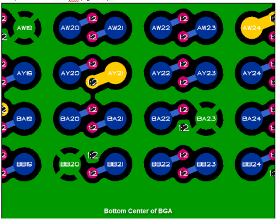
Example of swing breakout for a large 0.8 mm pitch BGA that includes surface ground fill.
High-Density PCB Design in Altium Designer
With the right design software, you’ll be able to define the trace geometry, via size, and layer stackup that you need to pack high functionality onto your board. Working with a design package that integrates your HDI circuit board design tools into a single interface gives you everything you need for HDI design in a single program.
Altium Designer Offers the Only Rules-Driven PCB Design Environment
As design rules are so important for ensuring manufacturability, you need a program that integrates your HDI circuit board layout features with online DRCs. In Altium Designer, the rules-driven design checks your HDI PCB layout against standard and custom design rules, which helps you spot and correct DFM errors quickly. You’ll have access to all this and more in a single design program. No other design program provides this level of consistency and productivity.
- Altium Designer’s rules-driven design engine in allows your design tools to be easily adapted to advanced circuit boards, including HDI PCB designs. Learn more about the rules-driven design environment in Altium Designer.
- Microvia design is an important aspect in any high-density PCB layout. Altium Designer gives you the tools you need to design microvias for your next HDI PCB. Learn more about microvia design in Altium Designer.
- You can easily adapt the design tools in Altium Designer to HDI PCB circuit board thanks to the underlying rules-driven design engine. You’ll be able to design your next high-density PCB layout to exacting industry standards. See how Altium Designer can be easily adapted to HDI design.
If you need to implement high-density PCB design and routing techniques in your PCB, you need a design platform that unifies your circuit board layout features with your design rules. Instead of using separate PCB programs with outdated workflows, you need to work in a single environment with all the tools you need. Watch as your HDI designs come to life with Altium Designer.
Altium Designer on Altium 365 delivers an unprecedented amount of integration to the electronics industry until now relegated to the world of software development, allowing designers to work from home and reach unprecedented levels of efficiency.
We have only scratched the surface of what is possible to do with Altium Designer on Altium 365. You can check the product page for a more in-depth feature description or one of the On-Demand Webinars.
