PCIe 5.0 Signal Integrity and Analysis

High-speed cluster computing, NVMe and SATAe, high-speed GPUs, AI in the data center and at the edge, 5G; they’re all using PCIe 5.0 to access computer peripherals. This standard and the upcoming Gen6 version of PCIe are pushing the limits of signal integrity for many computer systems designers, especially for systems to be deployed in a data center or edge environment.
As with any high speed signaling standard, signal integrity is a major design consideration, which requires the right set of design and analysis techniques. Rather than digging deep to find PCIe 5.0 signal integrity requirements from PCI-SIG, we’ve compiled the important points for today’s PCB layout engineers. Layout engineers should pay attention here as these design requirements will become more stringent in later PCIe generations.
PCIe 5.0 Signal Integrity Requirements
To begin, the requirements in PCIe 5.0 signal integrity do not translate to a strict set of board layout requirements; these will change depending on stackup, laminate type, weave style (if glass weave substrates are used), and other factors. That being said, there are strict requirements on PCIe 5.0 lanes to ensure signal integrity, prevent skew/ISI/jitter, and ensure a receiver can properly recover signals.
The table below lists some of the basic signal integrity requirements that apply in the PCIe 5.0 standard.
|
|
|
|
Loss budget |
Goal of 35 dB |
|
Signal bandwidth |
16 GHz per lane |
|
Vertical eye opening |
10 mV |
|
Horizontal eye opening |
0.3 UI (9.375 ps) |
|
Random jitter limit (RMS) |
0.15 ps |
|
BER target |
10-12 |
|
Impedance target |
85 Ohm differential impedance |
To get the longest possible lane while ensuring signals can be recovered at the receiver with low BER, interconnects need to be designed with minimized loss and impedance matching out to the farthest possible bandwidth. This is a difficult task in the presence of rough copper and dispersion in the substrate material. There’s also the matter of lane-to-lane skew, crosstalk, and design of receivers themselves with appropriate equalization.
Low-loss Materials
If you look through some of the current guides on PCIe 5.0 signal integrity and design, you’ll find some references to low-loss materials. However, there is no specific material defined in the standard to ensure signal integrity. The point here is to select a material that will ensure you’re within your insertion loss budget for your lane length, and everyone should agree that FR4 laminates are not the best material for long interconnects. Other viable options include Megtron, iSpeed, and Rogers laminates.
The Magic of Equalization
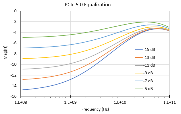
Equalization is an important part of PCIe 5.0 signal integrity as its job is to recover the signal seen at the receiver. The channel should be designed to the reference receiver specs, which uses CTLE+DFE (3 taps) to compensate for high-frequency loss with adjustable DC gain. The available equalizer gain under the PCIe 5.0 specification is shown in the graph below.

PCIe 5.0 equalization
Crosstalk, Skew, and Retimers
Dealing with crosstalk and skew is much easier thanks to the allowed use of retimers in a PCIe lane. These components are designed to retransmit a signal along a lane, thereby resetting the skew budget and insertion loss budget along a lane. This isn’t to say that crosstalk and skew aren’t important, rather you only need to worry about them up to the point where a lane meets retimer. You can learn more about retimers in this article from PCI-SIG.
Advanced Design Techniques Beyond PCIe 5.0
Once we get to PCIe 6.0, the requirements for which have already been determined mainly by PCI-SIG, we’ll get another performance bump to 64 GT/s with PAM-4 signaling. For the board designer, broadband design techniques will start to become even more important in order to minimize insertion/return loss and ensure signal integrity up to the receiver’s bandwidth.
Tools for this area of design and signal integrity analysis are more widely available today thanks to a wealth of electronics-specific field solver utilities, such as the Impedance Scanner in Ansys SIwave, as well as open-source optimization libraries, such as Sky Workflows. However, the real holy grail in design for interfaces like PCIe 5.0, USB 4.0, DDR5, and faster high speed signaling standards is the following:
- Design optimization. This is far superior to using a field solver for design, but it requires an analytical or numerical model that relates impedance to geometry. This was the subject of my recent IEEE EPS presentation, and I hope more designers take an interest as these techniques become part of high speed signaling standards.
- Design exploration. This basically brute-forces field solvers into an analytical approach. A great example is the new Simbeor 2021 package, which allows designers to explore multiple field solver solutions for proposed geometries in a real layout. This technique is much better for examining the effects of parasitics in a finished layout.
CAD tool vendors are always looking at more advanced field solver utilities they can incorporate into their products, so don’t be surprised if you start to see these more advanced methods used in your favorite PCB design software.
Once you’re prepared to address PCIe 5.0 signal integrity, you can use the high-speed design tools in Altium Designer® to create your high-speed PCB layout and model signal behavior with post-layout simulations. When you’re ready to share your work with your design team, you can share and track revisions through the Altium 365® platform.
We have only scratched the surface of what is possible to do with Altium Designer on Altium 365. You can check the product page for a more in-depth feature description or one of the On-Demand Webinars.
