PCB Ground Plane Best Practices in Your Multilayer Stackup

When I was first getting started with PCB design in modern CAD tools, I took a pretty simplistic view of grounding in my board. Coming into this industry as a physicist, I’m trained to think of things in terms of reference potentials, image charges, and any number of other terms from electromagnetic theory. Once you’ve gone through the effort to produce your first PCB, and you find aberrant noise and EMI in your design, the importance of clearly-defined grounds should become much more obvious.
Using a PCB ground plane in a stackup is the first step towards ensuring power and signal integrity, as well as keeping EMI low. However, there are some bad myths about ground planes that seem to persist, and I’ve seen highly experienced designers make some simple mistakes when defining grounds in their PCB layouts. If you’re interested in preventing excess emissions and ensuring signal integrity in your layout, follow these simple guidelines for implementing a PCB ground plane in your next board.
Why Use a PCB Ground Plane?
Before outlining how to use grounding and a PCB ground plane in your design, there are some important design goals that grounding will help you reach:
- Well-defined impedance: High-speed/high-frequency interconnects need to have well-defined impedance so that signals can interface with other components that have a specific system impedance (usually 50 Ohms).
- Return paths: A PCB ground plane provides a clear return path for current on an interconnect, which propagates as a displacement current in the ground region. This keeps loop inductance small and ensures low EMI emission, which is a major reason to use a ground plane or grounded copper pour in a multilayer PCB stackup.
- EMI shielding and suppression: EMI goes both ways, and grounded copper in your design can provide shielding against external sources of EMI.
- Decoupling and stable power: This is probably the least-understood reason for using a ground plane in a multilayer PCB. A pair of large power and ground planes will act like a big decoupling capacitor that helps keep power stable in the board.
There are a few cases where copper pour is used in sections instead of split planes, which can make it difficult to meet the design goals listed above. These problems with routing and keeping a well-defined ground plane can all create large loop inductance, which leads to EMI.
|
|
|
|
|
|
|
|
|
|
|
|
|
|
|
|
Note that, even if you have a uniform ground plane, a long return path can still form if a system is not laid out in a compact manner. There’s no need to have traces zig-zagging across the board, and having a uniform ground plane will not be the solution to your EMI problems in this case. Take a look at this example power regulator project from Mark Harris to learn more about this particular problem with return paths in a PCB.
How to Deal With Multiple Ground References
There are often times where you will have two different ground nets in your schematic, which will then be replicated on your PCB. As one example, this is common in galvanically isolated power converters (e.g., resonant LLC converters) and in many industrial Ethernet designs, where the high/low voltage sides or digital/analog sides of the system have their own ground regions. The ground regions are then tied back to each other with a 0 Ohm resistor or capacitor. Some people will recommend a ferrite bead here, I would be very careful with this due to the bandstop nature of ferrites.
If you have a board that requires multiple grounds, your PCB layout and routing strategy now requires considering where your true ground reference is at and how a return current is propagating into your reference net. This relates to points 1 and 2 in the above table, and it’s still common to see experienced designers follow an outdated design practice that creates EMI problems: splitting a ground plane into multiple regions of copper pour. Splitting your PCB ground plane in this way makes it difficult to define a clear return path, leading to large loop inductance, incorrect impedance, and radiated EMI.
Split Grounds and What Not to Do
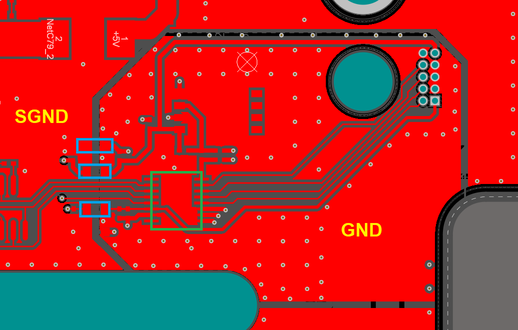
Consider the example layout shown below. In this example, we have two ground regions that are physically separated on the top layer. There are stitching vias that tie the GND region back to an identical polygon on layer 3, and there are other low-speed signals on layer 2.

The green component is a USB interface, and the blue components are capacitors tying the GND and SGND regions. If we were dealing with slower signals, we might be fine in terms of EMI as the parasitic loop inductance in this particular arrangement is not so huge. Since we’re dealing with USB, it’s better to play it safe and place a uniform ground plane below these regions. The lack of a ground plane below this gap in copper pour creates a differential impedance discontinuity and creates an excessively long return path through the capacitors. This return path will have high loop inductance, leading to greater EMI and susceptibility to crosstalk.
Tying Grounds Together
Personally, I would not worry about the capacitors and I would not separate the ground regions at all unless there was some reason for isolation in this type of system (e.g., low-voltage vs. high-voltage regions, operator safety concerns, some industry standard, etc.). Unless you need galvanic isolation AND you’re not designing high-speed return paths, you should just use a uniform ground plane. It’s also okay to run ground pour across the surface layer and tie it back to the main PCB ground plane. You’ll eliminate the radiated EMI problems you’ll see when routing over a gap in the ground plane, and you’ll ensure there is high isolation between different signals on the surface layer.
In summary, use a PCB ground plane when you need to provide a clear return path, and don’t place splits and gaps in the ground plane to create regions with different blocks of components. It takes some skill to ensure the return paths between different sections of the PCB do not overlap and create crosstalk. Read more about this issue with routing and return paths in a recent article from Francesco Poderico.
If for whatever reason you must use a star grounding strategy with different ground regions, do not under any circumstances start routing digital signals over the groundless region between your different ground plane regions. This is a recipe for strong radiated EMI and failed EMC testing.
When you need to place a PCB ground plane in your design, use the best set of CAD tools and the stackup design tools in Altium Designer®. When you’ve finished your design, and you want to release files to your manufacturer, the Altium 365™ platform makes it easy to collaborate and share your projects. We have only scratched the surface of what is possible to do with Altium Designer on Altium 365. You can check the product page for a more in-depth feature description or one of the On-Demand Webinars.
