
Low Noise, Low EMI Voltage Regulator
A couple of months ago, I purchased an entry-level cinematography camera: the Black Magic Ursa Mini Pro 4.6K G2. I'm planning to use it for project videos, factory tours, and trade show interviews with it mostly being mounted on a shoulder rig. In addition to the camera itself, this requires a surprising number of devices to be powered. To save having lots of batteries to keep track of, I want to run everything off the main camera battery. However, my experimentation with a cheap 5V 5A power supply from an online marketplace was less than satisfactory—so I'm going to design a purpose built low noise voltage regulator.
I'm not particularly experienced with operating cinematography equipment, but I have designed specialised hardware for very high-end aerial cinematography systems in the past, so I have some understanding of the requirements of systems on set, and the absolute need for zero down time-related to equipment. My regulator should meet the following high-level requirements:
Low noise: Because I'm running the regulator directly off the same battery as the camera, conducted noise back to the camera needs to be very low. The regulator will be supplying a brushless motor for the remote follow focus control, which creates quite a lot of electrical noise. As I don't know whether the camera has sufficient filtering built into the power input to deal with such noise, it's better to assume it does not, in order to not affect the analog circuitry within the camera. I'm also running two wireless RØDELink wireless microphone receivers - the power for these needs to be isolated to prevent a ground loop and any noise getting into the receiver. The first day I used the RØDELink running off my cheap regulator without isolation, there was a terrible hum on the audio, making it unusable.
High efficiency: As this will all be running from the camera battery, the regulator needs to be as efficient as possible. The camera and accessories' power demands are not insignificant, which requires me to carry around 600Wh of batteries for a single day of use. Every percentage of efficiency will be worth the effort.
Wide input range: I also have a monitor to run from the camera, which has a very wide input voltage range and can run directly off the battery without the need for separate regulation. I'd like to run it from a filtered supply to remove any conducted noise.
Finally, for requirements, I need to have the ability to move the camera from shoulder rig to either handheld or tripod mount with the minimum of fuss. My current system requires the unplugging of 3 power cables plus the SDI cable; if I was powering the RØDELink receivers, it would be 5 power cables, which are hardly a minimum amount of fuss. I can't do much about the SDI cable, but I can combine all of the power cables into one harness/plug which can then go to a distribution board on the shoulder rig, leaving me just two cables to remove from the camera and remember to plug back in, which will save a lot of time.
My requirements for this project are:
- 12-17V input
- 5V, 5A total supply, load spikes up to 1A over average,
- Two isolated 5V outputs with a minimum of 260mA each,
- Single plug with 5V, battery voltage, and filtered battery voltage,
- Filtered battery voltage that is capable of a minimum of 1A load, preferably 3A,
- Low radiated noise,
- Low conducted noise,
- Low voltage/current ripple
That's quite a list, so I'm going with a typical cinematography approach of "money is no object." Cinematography gear is crazy expensive, but also very reliable and expected to do everything advertised and then some. As there's nothing on the market that can meet my needs, I'm expecting to spend a bit of money on this project's components, but still have it be one of the cheaper components on the camera/rig. At the end of this project, the BOM came to about $57 each at 10 units quantity or $66 in singles. ActiveBOM shaved about $8 off each unit at the 10 qty in price by shopping around for me, which i was pretty impressed with. While this may be an expensive power supply by most people's consideration, the cost of the components, board, and enclosure for a single unit is still going to be cheaper than the Smallrig side plate, which this project is replacing!
In this article, I'm only covering the regulator board's design, which will mount to the camera itself. The shoulder rig mounted board is just a breakout board only consisting of connectors, so it isn't of much interest to cover here. As always, this project is available on GitHub under the permissible MIT license. You can download it to use as the basis for your own project or to use directly. I'm using my Celestial Altium Library for the components on this project, as usual. The accurate 3D models in my library really help with mechanical integrations such as this project.

Above is the PCB design you'll be reading about in the Altium 365 Viewer; a free way to connect with your co-workers, clients, and friends with the ability to view the design or download with the single click of a button! Upload your design in a matter of seconds and have an interactive way to take an in-depth look without any bulky software or computer power.
Mounting and Enclosure Design
One of the challenges with a project such as this is figuring out where the device will go that will make it be useful rather than just getting in the way. I have a Smallrig side plate on the side of my camera that has my two radio receivers mounted on it.
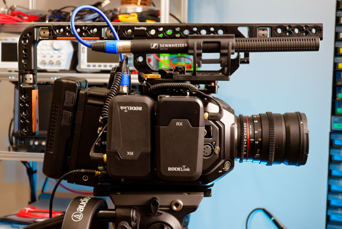
I have a friend with a high quality CNC vertical mill. He will be making me a new side plate that will also be the enclosure for the control board. The side plate isn't quite made to hold two receivers, so I'd like to make my housing capable of handling both receivers (mounted on a standard cold shoe) directly.
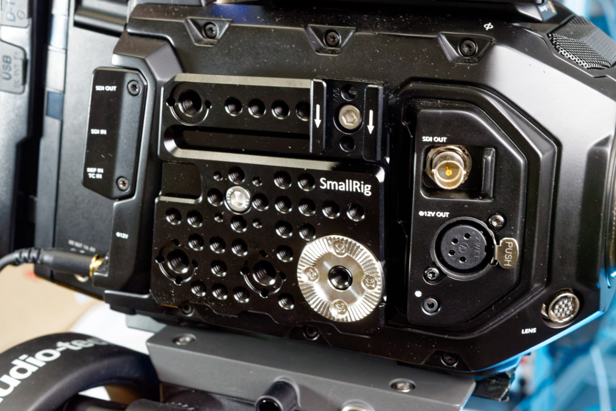
I'll be referencing the Smallrig side plate for the measurements for mounting my own enclosure. The camera side has an ARRI Rosette mount, which is designed for mounting accessories to and will form the basis for my mounting solution.
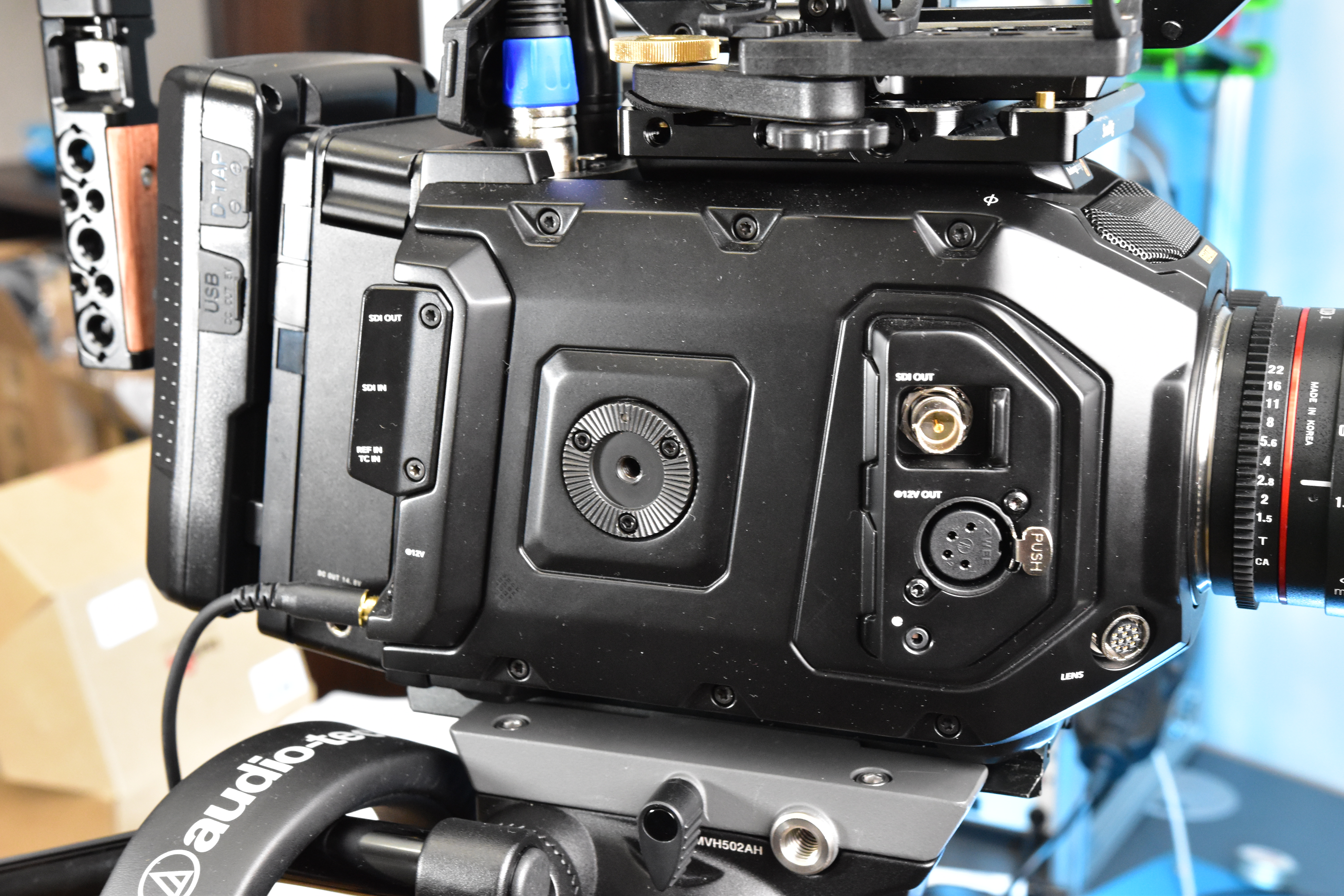
Before getting into the project's electronic design, I first need a board shape to determine how much area I have to play with and allow the layout of components.
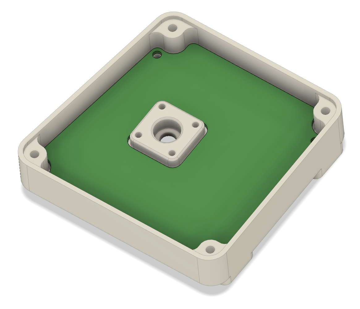
With a little work in a mechanical CAD package, I have the basics of an enclosure designed. The centre square boss is where the rosette mount on the camera is. Rather than machining the rosette directly into the enclosure, I'll buy a stainless steel mount similar to what can be seen on the Smallrig plate. This boss allows sufficient thread depth for the mounting plate, as well as the bolt head. There is some extra material under the PCB where the boss is, as this point will have the highest stress during transport and perhaps even use - this area will provide some central PCB support as well due to this. I have 4 mounting screws for the circuit board, as well as extended corners in the enclosure for mounting the top lid too, which will have the cold shoes for the radio receivers.
This will be a very solid case and should help to contain any radiated interference from the board, even with some cutouts for airflow. The significant thermal mass will also make for a good heatsink, not that a highly efficient regulator should need a lot of heat to be dissipated.
Choosing Major Components for the Low Noise Voltage Regulator
Now that we have an enclosure designed and a board area defined, we can start looking at the project's component options. I'm mostly looking for what will give me the highest simulated power quality without taking up too much space. Vertical height, especially for capacitors, is a factor to consider. More height will just push weight further out from the camera centreline, which could make things uncomfortable or awkward on the shoulder rig.
Regulator IC
The voltage regulator is the most critical component for this project, so it makes sense to start with it. I simulated regulators from Texas Instruments, STMicroelectronics, and Analog Devices. The Analog Devices LTC7151S from the Silent Switcher 2 series was impossible to beat. My simulated design is around 98.5% efficient at a nominal load and voltage, which is seriously impressive. The cost is higher than other options for the IC itself; however, it is a tremendously powerful monolithic device which does not require external MOSFETs - the total solution cost was very comparable to the other options I was evaluating. In addition to the excellent efficiency, it's also advertised as having low EMI operation. It checks all the boxes and has a lot of headroom for additional current if required in the future.
Isolated Regulator
In a previous project, I designed a USB isolator to protect a computer's USB inputs from mishaps with dev kits and prototype boards. My isolated outputs for these projects are going to copy that design, and use the Murata NXE2S series of isolated regulators. I can't design a smaller isolated supply than these, and other options available from other suppliers have higher noise and/or lower efficiency. These are not super efficient, but they are only supplying the radio receivers, which draw around 260mA each. My main concern for efficiency is the other accessories that consume a lot more current. With appropriate filtering, the noise output from the regulator is acceptable for my RØDELink devices.
Connectors
For the input connector, I'm going to use a barrel jack. I'm not a fan of barrel jacks. However, it is very common to find D-Tap to barrel jack connectors in the cinematography world. The D-Tap connector is a type that only really exists in cinematography applications that I've found, and each battery has an output connector, as does the camera body itself. As this is an open source project, I'd like to make it usable for other people too, without needing specialised crimping tools. The barrel jack's location on the device should prevent it from snagging on anything and accidentally pulling loose.
In addition to the two isolated USB type A ports for the radio microphones, I'm going to provide a non-isolated USB type A port on the device for future use. I don't currently use it, but my camera rigging is constantly evolving, so I may soon find a need for an extra USB port on the camera itself.
Finally, I decided to use a Molex Micro-Fit 3.0 connector to supply power to my shoulder-rig distribution board for the connectors. The Micro-Fit connector met several requirements for me, primarily the current capacity and availability of cables. Molex sells pre-made cables for the Micro-Fit series in 150mm, 300mm, and longer lengths - the 300mm length should be perfect for my shoulder rig attachment. The contacts are rated for 5A, which is exactly what I need, and it's a latching connector without being too much hassle to connect and disconnect - both giving it bonus points. The small size of a 3x2 connector is also very desirable.
Power Indication
To diagnose faults quickly, I want to have a power LED for input as well as the main regulator and each isolated output. What I learned from my cheap 5V regulator is that it's critical not to have any LEDs facing forwards from the camera - even an LED covered in black hot melt glue will still show a reflection on a machine enclosure or glass which is very undesirable. I'm going to use light pipes to show a power indication next to each isolated USB port and have a light pipe on either side of the barrel jack, which will show the input power, and the main 5V regulator is working. As an advantage of not wanting to much light out of these, I'm able to use very cheap LEDs and run them a very low current, so you'll be able to tell that the device is working, without creating reflections or impacting the colour balance of a scene.
The light pipes will make looking at the LED status very easy, as they will bring the light directly to the side of the enclosure allowing a less powerful LED to be visible. For cinematography gear, LED indicators need to be discrete and dim, yet still easily visible - a hard balance to make.
Designing the 5V, 5A Low Noise Voltage Regulator
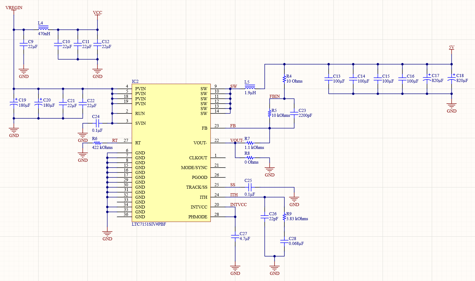
I have selected the Analog Devices LTC7151S to base the design around, as mentioned above it's a very powerful monolithic regulator capable of driving up to a 15A load. I'm designing for a maximum 5A load, with a nominal load of around 3A. However, my high efficiency requirement will typically mean I'm using oversized inductors to keep the series resistance low, and the oversized capacitance for low voltage ripple means that this design should be more than capable of supply significantly higher loads with only a slight drop in efficiency. The large metal enclosure and significant copper area on the board will also help dissipate the extra heat from higher current loads than designed. My simulation expects the design to be over 98% efficient up to 8A load, at which point the junction temperature of the regulator will reach about 87C at 25C ambient - that does not factor in the hefty aluminium housing, however. The design is stable for the full 15A load. The PCB design for this project would be appropriate for this high load, as the conductors to the connector pins, and the connectors themselves are not sufficient for this current draw.
Knowing that I want the highest efficiency possible, I am running the regulator at the minimum frequency it can operate it, 400kHz. This will mean my inductor and capacitor components are going to be quite large for the current load placed on the regulator, but with the board space I have, it's a tradeoff I'm more than willing to make.
Inductor Choice
With my 5A load, I expect the peak inductor current to be approximately 7.12A, and at the peak supply current the regulator is capable of, the current would be 18A. Using the formula in the datasheet, I should be aiming for a 1.79uH inductor. With my extreme efficiency goal, I chose a Würth Elektronik 7443556190 inductor, which is quite large and capable of a continuous current of 32.5A - the 1.2mOhm DC resistance (DCR) is the main reason behind the selection of this component.
Inductor choices with lower DC resistance for a suitable inductance value were all significantly larger, and more importantly, significantly taller with a very small change in DC resistance as a tradeoff. The Würth part has an inductance of 1.9uH, which is very close to the ideal value.
Capacitor Choice
The regulator's capacitors with a 5A load will need to deal with 2.4A RMS of current according to the formula in the datasheet. To keep efficiency up and loss down, for my input ceramic capacitors, I chose to use two 22uF capacitors with the lowest ESR I could find, which means they come in a rather enormous 2220 imperial (5750 metric) package. The specs of these capacitors mean I have around 17.6uF of usable capacitance per capacitor - by comparison, a high quality 1206/1210 sized capacitor only offers about 4-9uF of actual capacitance in the design. The much larger footprint is cheaper and offers a higher capacitance per mm2 of the PCB area.
The bulk input capacitance is provided by a pair of 180uF aluminium polymer capacitors, also chosen for their low ESR. The output capacitance is provided by 4 low inductance, low resistance 100uF ceramic capacitors, also in the 2220 imperial package. The bulk output capacitors are two 470uF aluminium polymer capacitors. The output capacitance simulates as providing just under 2mV p-p ripple, or 0.019% of the output voltage, which I'm very happy with.
Input Filter
I've said in project articles before, and I'll happily say it again - input filtering for a switched mode power supply is just as critical for many applications as the output filtering. I'm using a simple Pi filter for the input filter on this project, but it's incredibly effective at reducing the amount of conducted emissions.
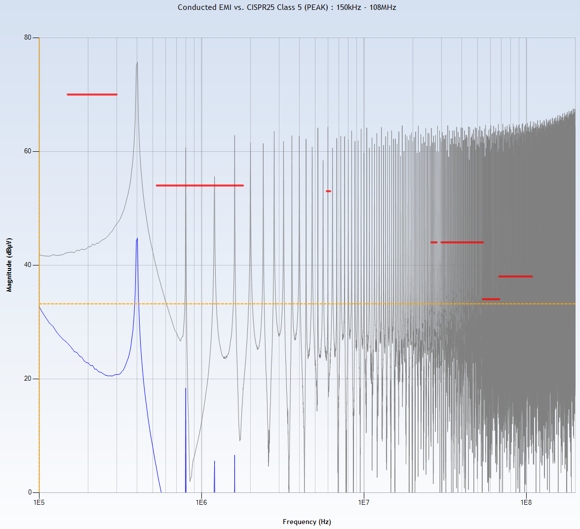
This is a simulation of the conducted noise with the CISPR25 Class 5 limits displayed as red bars. The magnitude of conducted noise is displayed in grey without the filter. With the filter is displayed in blue, with the plot rapidly dropping off the graph. The large spike is, of course, 400kHz, the regulators operating frequency, and the subsequent spikes are the harmonics of the operating frequency.
However, this design does not need to conform to automotive specifications, however, plotting against CISPR25 gives us a nice visual representation of what is acceptable. With the input filter in the design, very little noise will make it through to the camera to disturb its analog circuitry compared to an unfiltered input.
The input filter is a simply another pair of 22uF 2220 imperial sized capacitors plus a smaller 22uF 1210 capacitor thrown in for good measure. An extra 22uF 1210 capacitor is used in addition to the input capacitors for the regulator to complete the Pi filter. I chose a 480nH Würth Elektronik 744309047 inductor primarily for it's low DC Resistance. It's far more inductance than is strictly necessary to clean up the conducted emissions. The large inductor is overkill, but at the time of design, I felt as though I had the board space to justify the use of a large inductor package allowing me to gain a lot of inductance whilst keeping the DC Resistance low.
Battery Voltage Filtering
At the start of the article, I mentioned that I would be looking to have a filtered output for my display and any other battery voltage accessories. To keep my bill of materials simple, my battery voltage filter is identical to the voltage regulator's input filter. The inductor for the filter is more than sufficient for whatever my accessories can throw at it, and will mitigate any harmful noise from the camera's power input.
ESD Protection
I have to admit here that I completely forgot about ESD protection on this design, I was so focused on a low noise voltage regulator and power supply that I neglected to consider ESD! Luckily, one of the members of my library's discord channel was talking about ESD protection as I was doing the layout of this project and it reminded me of the need. While the regulator IC itself should handle an ESD event without a problem, and the relatively large capacitance and inductors of this design should also help mitigate an ESD event, I'm always a big fan of making a design the best you possibly can.
I added TVS diodes to the board's connectors to ensure the power rail will have some clamping for high transient voltages. The member of my library community who was talking about ESD suggested that I use the Texas Instruments TPD1E10B06QDPYRQ1 for my USB connectors since I had very little board space left to play with around the connectors. Its 0402 package was well suited to sitting right on a USB Type A connector's voltage pin. It should be more than capable of handling a typical shock. I'm using slightly larger SOD-123F didoes for protection on the main connector. This connector is going to a power distribution board that has more change of being touched and will see more plug/unplug cycles than the USB connectors. The SOD-123F package is capable of handling more than twice the discharge of the small 0402 diodes.
For the main power input to the board, I decided to go with something a bit larger than the 5V connectors. I would hope that most of the 5V devices have their own ESD protection that would also be mitigating any voltage buildup on their cables - however, I don't expect the same from the battery. If the camera battery has just been pulled from a pocket in a low humidity environment, it could have quite a charge on the plastic body. If my power device is plugged into the D-Tap connector directly on the camera, rather than the camera body, that charge may still exist by the time my device is plugged in. The shock would be larger than a typical human body model discharge. To handle this higher energy discharge, I decided to go with a Bourns SMAJ18A in an SMA size package. This will handle a 400W discharge over the 90W the 0402 sized diodes capable of withstanding and clamp the voltage below the maximum that the Analog Devices LTC7151S can withstand.
Board Layout and Design
I exported my PCB shape from the mechanical CAD design as a STEP model, which makes it very easy to import into Altium. I really love Altium's ability to take a 3d model of a board shape and turn it into a board outline. For projects like this where you fit a board into an odd enclosure, it's invaluable.
You can define the board shape from a 3D mode by going to design -> Board Shape -> Define from 3D body when in the 3d view mode of the PCB editor. Just click on the 3D body and then on the face to use as the outline.
.png)
With a few clicks, I have my board shape imported.
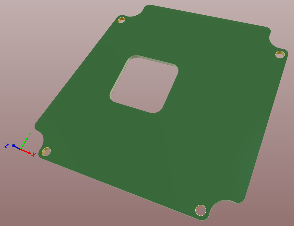
I have to admit, after adding all my components to the board I had a bit of sinking feeling thinking that perhaps all my design choices based on "I have lots of PCB space" were perhaps a bit unjustified. Often I feel this when trying to work on a small design and see a huge array of components to fit onto the board, but its usually worse than it looks.
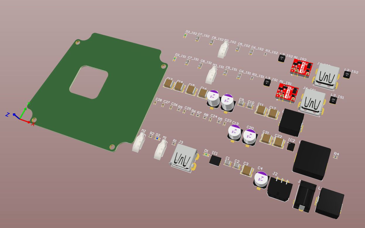
To try to figure out if I had used more large components than my board could handle, I started off with the connectors. These are going to be in fairly specific locations, as the isolated USB ports must be at the top of the device. The connector for the shoulder rig breakout board must be on the front edge in a location that won't interfere with front SDI output or LANC input connector, and the power input needs to be at the back to make cabling easy.
I'm going to show a few more of the PCB layout process steps here than I normally would. I have had several students tell me that when I have done this in past projects, it has been very helpful to them, by giving some insight into the thought process that goes into a PCB layout.
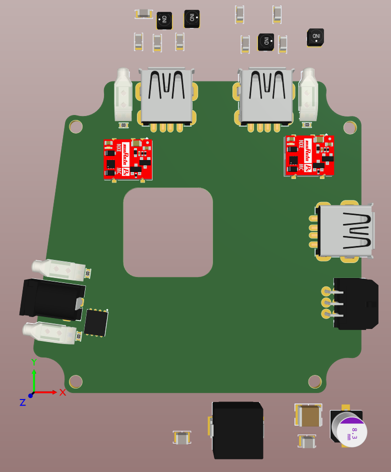
Next up is the challenge of trying to fit all the rather large inductors and a large number of bulky capacitors onto the board in a manner that makes sense electrically. I decided to add the isolated 5v supplies to the board, and then get an idea of how the battery voltage filter might layout. This would give me a better idea of available board space. The isolated supplies would be ideally mounted very close to the point of load, the USB connectors, and they fit very nicely at the board's top.
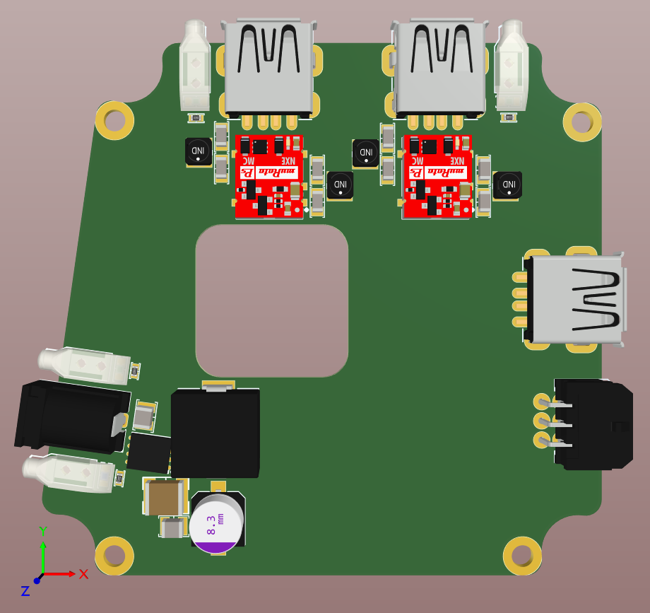
After that, my strategy for this was to create an optimal layout off the board area for the regulator and then see how I'd be able to fit that on the remaining board area.
The LTC7151S is slightly different from a typical regulator in that it has input voltage pins on both sides of the package, rather than just a cluster on one side. This adds additional challenges to the layout, as input capacitors are required on both sides of the device as well as the need to get power to both sets of pins/capacitors.
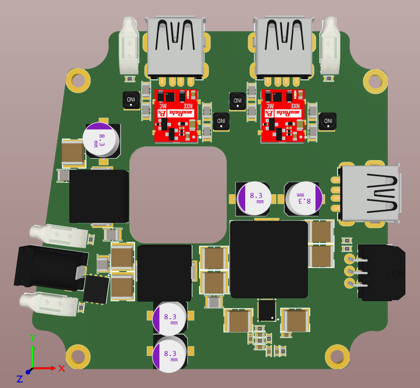
Bringing the regulator onto the board proved that everything would fit, but the layout was less than ideal. I had to move the battery voltage filter above the input connector. It just wasn't looking great - the voltage regulator also had it's bulk capacitance all on one side, rather than being more ideally balanced between the two inputs.
Balancing the input capacitance to the regulator was my next goal, along with trying to clean up the input filter.
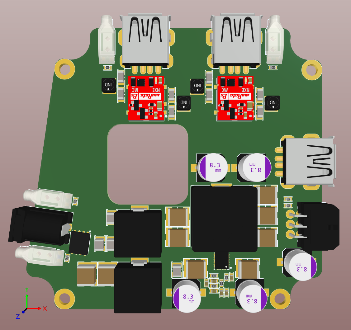
I managed to get the voltage regulator looking somewhat cleaner, and moved a couple of the battery voltage capacitors over to the output connector - but this isn't ideal for filtering.
After playing with this layout for far too long, I grabbed my calipers and started measuring the camera to see exactly how far up the board, I could place the barrel jack. The camera has a raised section for the rear SDI connector right next to where the board would be, and I didn't want to get stuck not being able to plug the barrel jack in. Going back and forth between the mechanical model and the camera, I found that the barrel jack could actually go anywhere along that side of the board without causing an issue. In hindsight, I should have started looking at the camera a lot sooner than I did.
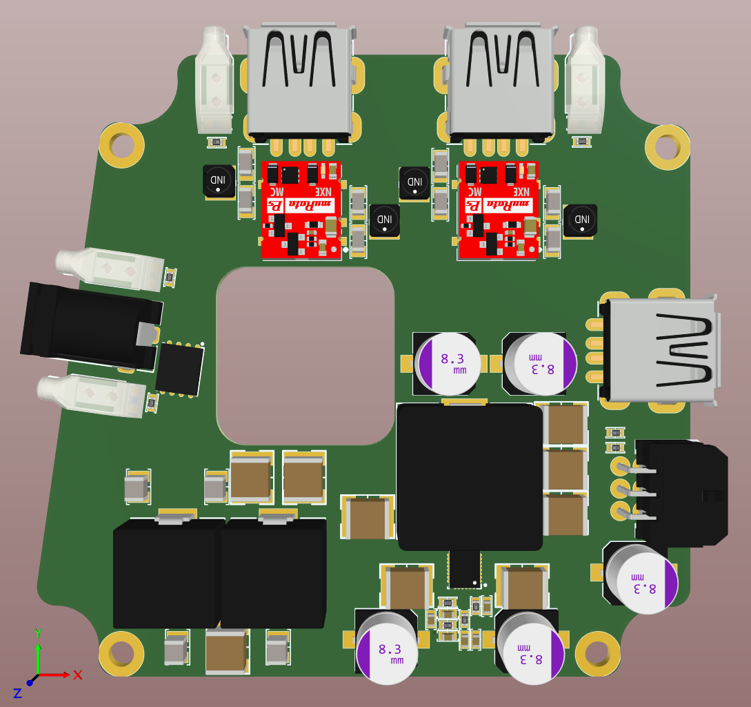
With the move of the barrel jack up the board, it was looking a lot cleaner, but I still had the output capacitors for the battery voltage filter over near the connector. At about this point, I realised I had completely neglected to add any ESD protection, which threatened to throw my whole layout out the window again.
Thankfully, I was able to find some ideally sized diodes for protection, and continue the layout. I moved the output capacitors for the battery voltage filter over with the rest of the filter block at this point, making use of the free space on the left. I wanted to keep the two inductors of the two input filters side by side, as it allowed some sharing of the input capacitance and made routing of the input voltage quite optimal. The two inductors side by side were much more optimal for routing of the power than the 'one above the other' in the previous rough layout.
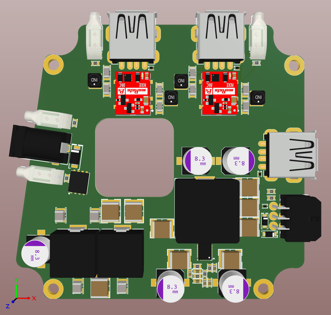
Finally, this looked like a board that would be worth routing. This board has no routing performed yet, so you can play spot the difference between this screenshot and the one below to see how things moved to try to fit conductors on the board.
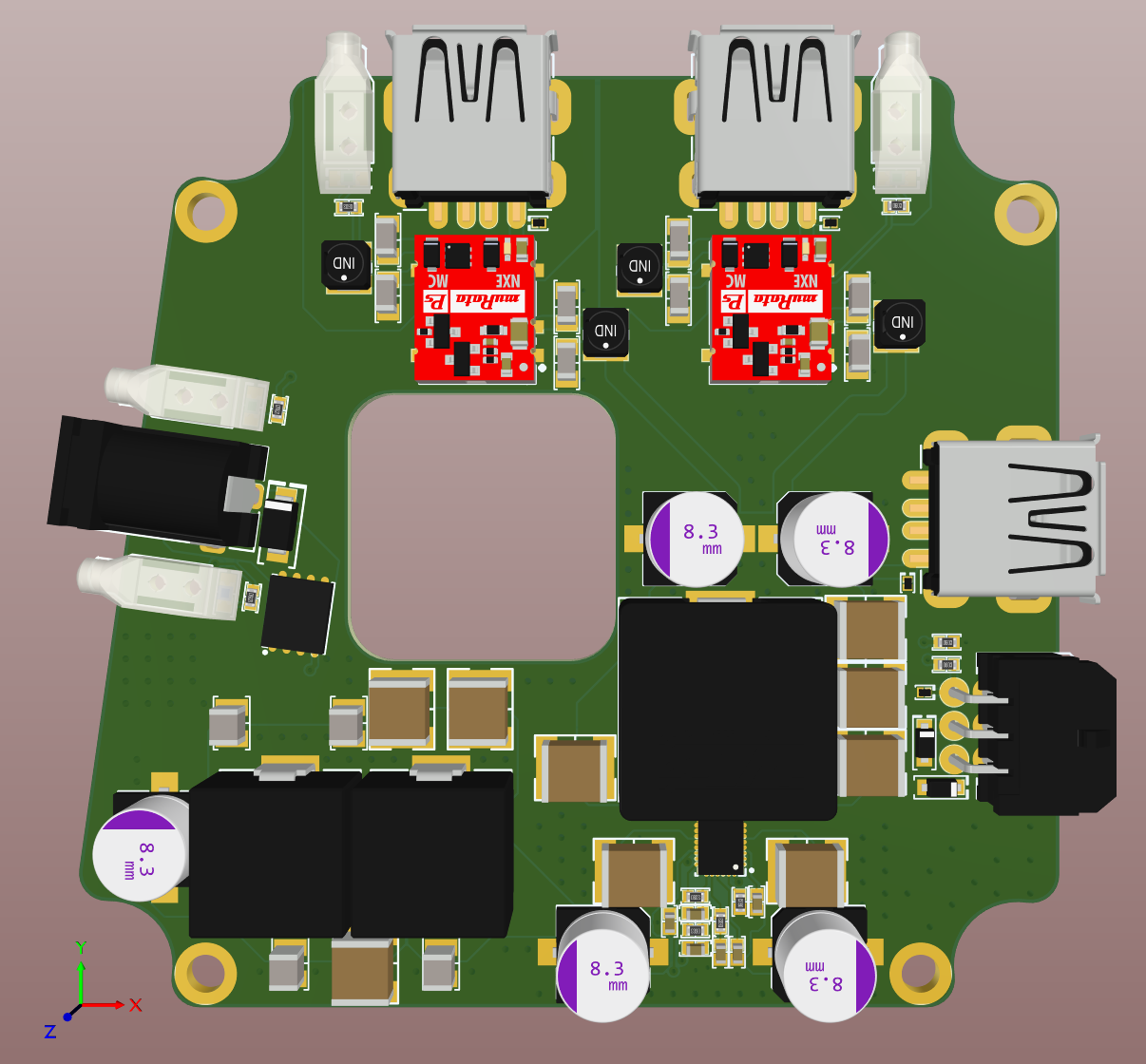
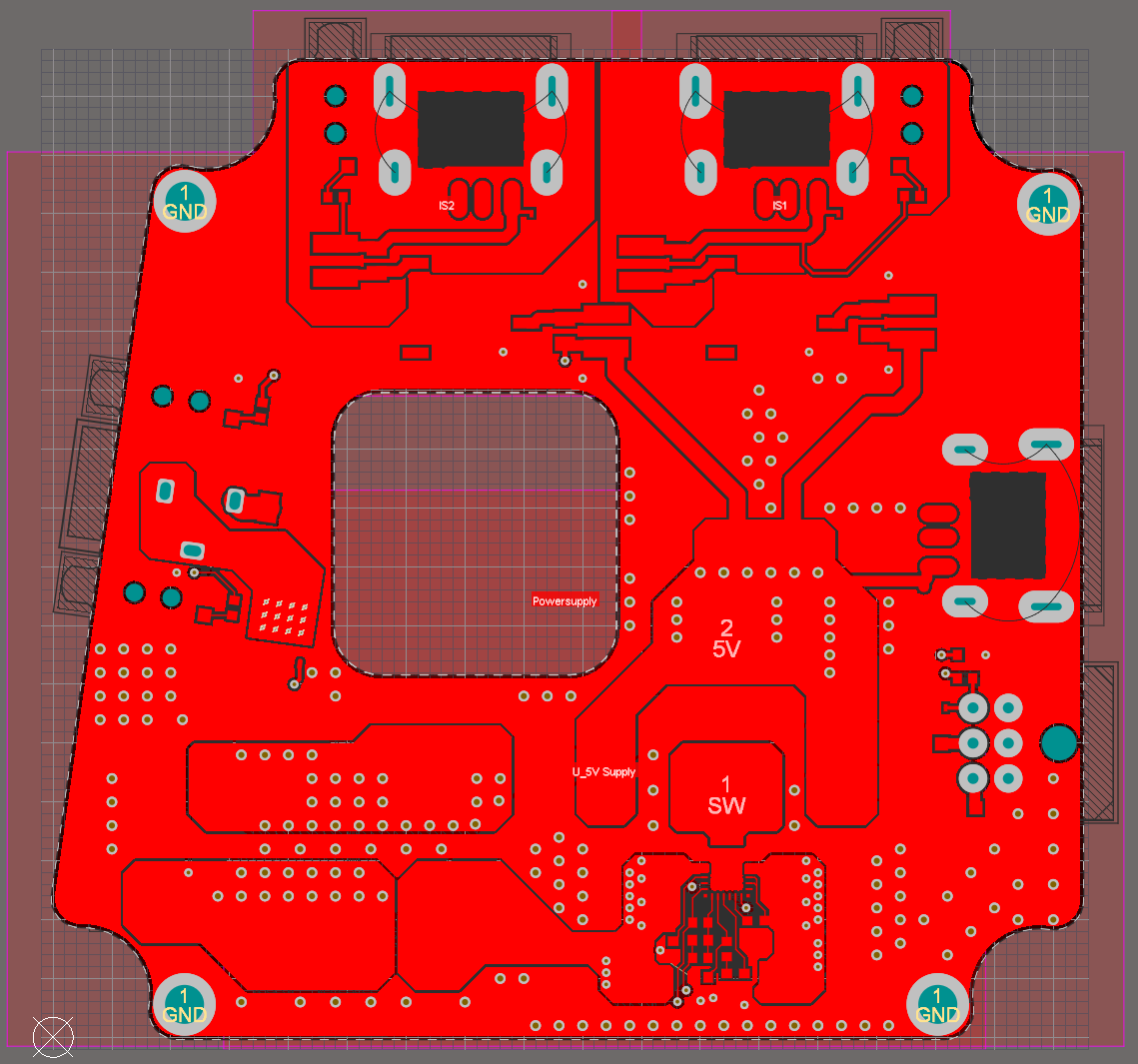
There was no real advantage to trying to keep the power conductors on one side of the board over the other for many locations through hole connectors on the input and output. Therefore, I used the bottom of the board for most of the power runs.
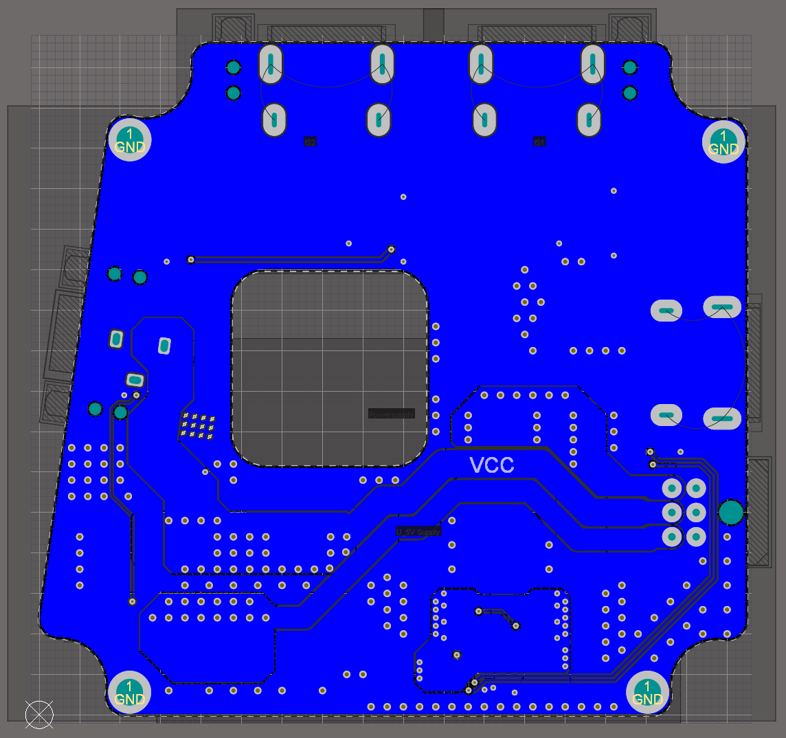
I will say that this is not ideal from the TVS diode protection standpoint, as the diode should be on the trace between the connector and the source/load, not separate to it. With the board space available and not wanting to go to a double-sided component board just for 3 diodes (requiring a second stencil, second assembly job, second reflow), I decided to go with the less-optimal ESD protection layout.
The battery voltage passthrough and filtered battery voltage should not be affected by an ESD event, as there are no sensitive components except the electrolytic capacitors. The ESD protection on the battery voltage lines is mostly for protecting the camera and the regulator input. The regulator IC has enough capacitance and inductance on both the input and output, as well as good ESD rating itself that I feel comfortable with the 'less than best practice' placement of the diodes, and that the board would pass CE testing for ESD protection as it stands.
Finishing the Enclosure
With my PCB routed, I need to turn the enclosure design's rough layout into an actual machinable enclosure, with a top. Ideally, I'd be using a professional mechanical CAD package such as SolidWorks, Creo, or Inventor rather than Fusion360 - this combined with Concord Pro would give me a lot better experience with the MCAD-ECAD interface. I don't do enough mechanical CAD work to justify a professional MCAD package's cost, so I need to do things the old fashioned way!
There are two options for working with other MCAD software when it comes to 3D modeling/integration, STEP or Parasolid. The STEP models are simpler, and they do not include any copper, and the board does not include vias. Parasolid can make your computer slightly stressed as the level of detail of the export is quite high, including all the PCB layers, copper, and such, which generates many elements for the CAD package to deal with. For some integrations, this detail level is absolutely necessary - however, for what I'm doing, a STEP model is sufficient.
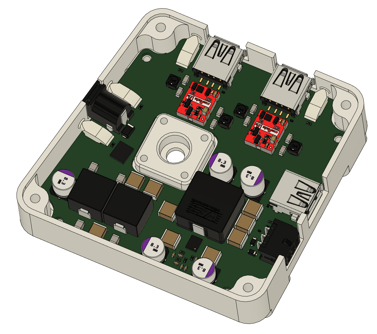
With my STEP model exported from Altium and imported in the Fusion, I can align the exported board with the mounting points and create my connectors' enclosure cutouts. With the 3D model, I was also able to create a boss on the enclosure under the regulator extending out to the regulator's inductor, which can be used as a heatsink - not that the regulator is expected to get particularly hot under it's designed load.
For the top of the enclosure, I added my two cold shoes for mounting the microphone receivers. The placement is such that the two receivers stay in the photos' orientation earlier in the article. They should be level with each other both on the top and bottom as well as in how far they stick out from the camera, which is an improvement over my current side plate. I have also added another position for an ARRI Rosette which could be useful in the future, or perhaps to other users.
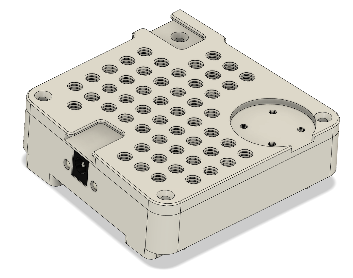
To finish the top part of the enclosure off, I added a grid of 1/4-20 UNC tapped holes, which will allow many configuration options in the future as my camera rigging system evolves. This also allows some airflow within the enclosure, further enhancing the cooling capabilities of the design.
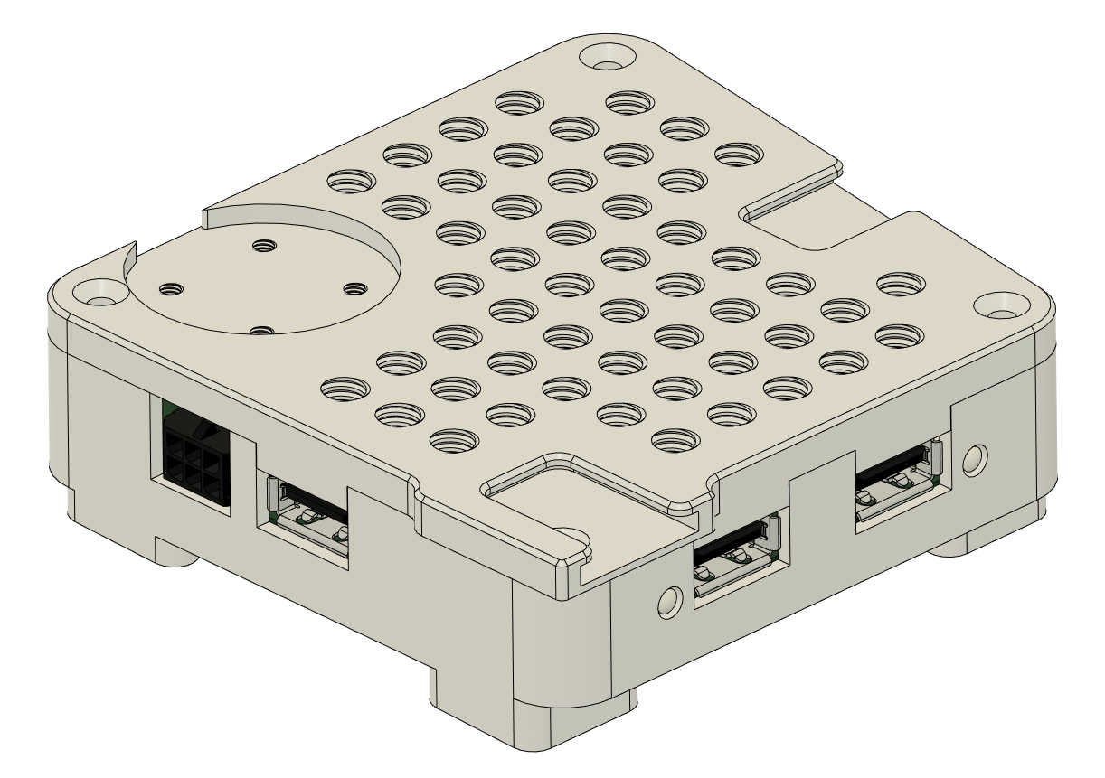
The top part of the enclosure will extend down over the USB connectors to provide a finished enclosure.
Finally
Hopefully, this low noise voltage regulator project has provided some insight into the design and layout process when working with an enclosure and odd-shaped board. You can find the PCB design files and schematic for this project on GitHub. The design is free and open source, licensed under the MIT license.
Would you like to find out more about how Altium can help you with your next PCB design? Talk to an expert at Altium.