Altium Rigid-flex Guidebook: Your Complete Design Guide

Many electronic devices don’t live on a single printed circuit board. Flex and rigid-flex PCBs are used to link multiple rigid PCBs together into a single unit. This allows printed circuit designers to customize their board to odd enclosures, design motion into new devices, and provides unique form factors that are not possible with rigid boards. Many other common devices are shrinking, and the PCBs that power them are following suit.
If you’re looking for the best PCB design software for your next device, you need a platform that integrates all these design aspects and more into a single software package. Altium Designer is the only PCB design software package that gives you the tools you need for flex and rigid-flex PCB assembly and design in a single platform. Instead of using other design platforms that silo important features, you can take a new flex printed circuit design through to production with Altium Designer. Take a look at our rigid flex PCB design guidelines below to see how you can design successfully with Altium Designer.
ALTIUM DESIGNER
A printed circuit board design software package that allows full customization of your next flex or rigid-flex board.
PCBs have infiltrated every aspect of our lives, and more advanced designs require creative methods for placing required functionality in a single device. PCB designers need to be familiar with numerous techniques and design rules in order to keep up. With wearables, IoT, mobile, and odd-shaped devices being ubiquitous, it pays to understand flex and rigid-flex PCB design techniques.
Many electronic devices don’t live on a single PCB. Rigid-flex PCBs are used to link multiple rigid PCBs together into a single unit. This can improve the adaptability of your PCBs and allows PCB designers to customize their board to odd packaging. Many other common devices are shrinking, and the PCBs that run them are following suit. If you are looking for the best PCB design software for your next device, you need a platform that integrates all these design aspects and more into a single software package.
Flex And Rigid-Flex Design Challenges
Flex and rigid-flex PCBs come with their own set of design challenges. Routing between multiple boards on a rigid-flex PCB spreads your components over a large area, and your enclosure needs to be designed alongside the mechanical shape of your board. Your device application and form factor require you to consider whether your flex elements will be static, dynamic, or creased. Each of these options comes with its own set of design techniques.
Static flexible PCB ribbons are set in place on the board and are not intended to move (or move very little) when the end product is used. Static flex ribbons are not always creased, they may simply have a slight bend that allows each end of the board to fit in its packaging. Dynamic flex ribbons are intended to bend and move with the device enclosure, but the flex PCB ribbon should not permanently deform during operation. The image below shows an example of a board with static ribbons.
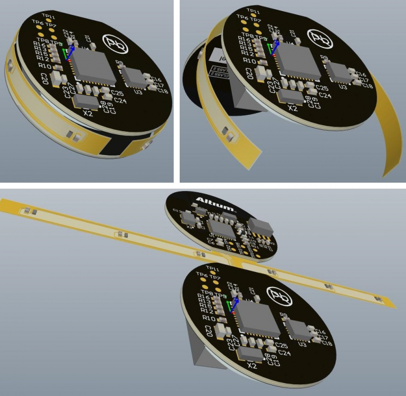
Your flex or rigid-flex PCBs carry strict mechanical constraints alongside important electrical requirements.
In the above image, the backside of the flex board may be permanently deformed and creased so that the final board keeps its shape. Creased flex PCB ribbons are static flex ribbons that are permanently deformed, and this deformation is applied during PCB manufacturing and assembly.
Choosing Between Rigid, Flex, or Rigid-flex PCB Design
Your standard rigid board only lets you design in two dimensions, whereas flex and rigid-flex printed circuit design can be made three dimensional. You can design your electronic device with odd form factor and with interesting new applications in mind. When you’re planning your next electronic medical device, IoT product, or wearable, it pays to know when it’s best to use a flex, rigid-flex, or rigid PCB.
What are Flex Circuits?
PCBs are built to be rigid, rigid-flex or flex according to their implementation and application. By far, rigid printed circuit boards are the most problematic as the boards may break during manufacturing or handling. For other boards like rigid flex and flex circuit boards, including some that may be utilized in aerospace systems, a specific degree of flexibility or rigidity is required. Whether rigid-flex or flex, PCBs must adhere to IPC 6013-D, as well as mandatory regulatory requirements for quality according to AS9100D, and reliability as stipulated by IPC-6011.
A well-known commercial example is for wearable electronics that include fitness and health monitors. Flexible printed circuit boards for aerospace systems are used to provide thermal stability, increase reliability, simplified assembly, and lower costs. Another usage being envisioned is foldable wearables, which can be used to monitor vital signs, as conformal heating elements, and as medical devices.
Rigid-flex vs. Rigid Printed Circuit Board Design
If you know your new product will need to partially bend, flex, or fold, you’ll likely need to use flex circuits and/or rigid-flex boards for your new product. Most present-day designs require several signal layers within your rigid PCB, and using a rigid-flex board will still allow you to use multiple signal layers while complying with your mechanical requirements.
The additional design considerations for flex circuits and rigid-flex circuits may include board materials, vias, and thermal management, which can test the limits of some PCB design programs. However, with Altium Designer, designing rigid-flex boards is easy.
- Making the right design choices requires weighing the trade-offs between flex and rigid-flex PCB design. If you’re working on the latest and greatest IoT and wearables, it pays to know when to use each type of PCB. Learn more about the tradeoffs between flex circuits and rigid-flex PCBs.
- Rigid-flex and flex PCBs have been around for some time, but flex PCBs are set to be the wave of the future, especially in wearable devices. Learn more about how flex PCBs are taking over.
- Not all designers or engineers are familiar with flex and rigid-flex design, but the right design software and techniques will help you be successful. Learn more about design techniques for flexible circuits and rigid-flex PCBs.
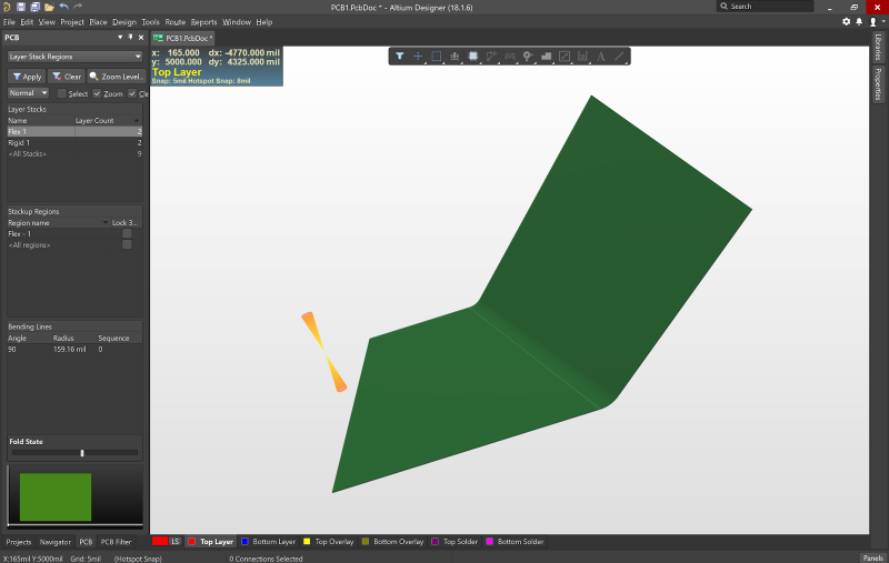
You’ll need to define your bend regions as you create a layout strategy for your board.
Layer Stackup In Rigid-Flex and Flexible Printed Circuit Boards
Your flex circuits and rigid-flex circuit boards will still have sections built up from common rigid PCB laminates. The most common rigid insulation material is called FR4. It is an industry designation that represents the ratio of fiber to resin, so materials may vary somewhat to meet FR4 resin content and glass weave requirements. For specialized applications, such as radio frequency or mmWave designs, other types of material designations are available. Consult IPC-2221 for listing of all PCB material types.
The ribbon in a flex or rigid-flex PCB is made from flexible polyimide, where traces are routed only in the internal flexible layers. The rigid PCB ends of the board are multilayer structures, and traces are routed across the flex ribbon between rigid sections. In some boards, the flexible circuit ribbon also has multiple layers, and a plane layer can be routed across a flex ribbon.
Implement the Best Layer Stackup Strategies in your PCB Design Software
With so much activity happening below the surface of your PCB, your design software should help you keep track of it all. You’ll need design tools that let you define a full layer stackup and the link between layers in a rigid-flex device. Your design software shouldn’t be limited to working with FR4, you need design software that lets you customize everything from board footprint to your layer stack. A great PCB design software package will include a full layer stack manager that shows a graphical representation of your layer arrangement and the links between boards in a flex or rigid-flex PCB.
- Rigid-flex design can be much easier when you design within a board outline. Learning the best design techniques now can save time on redesigns later. Learn more about designing your next rigid-flex PCB from a board outline.
- You’ll need to define outlines for your flex and rigid PCB regions, but you’ll also need to integrate these reasons with the right stackup. You can easily include a flexible polyimide ribbon in your board with the right layer stackup design features.Learn more about designing a layer stackup for a flexible or rigid-flex PCB.
- When planning your stackup, you’ll need to decide whether your board will have static or dynamic flex regions. The right bending radius required for each type of flex region for your flex ribbon depends on the stackup within the flexible ribbon. Learn more about static and dynamic mechanical requirements for flex PCB design.
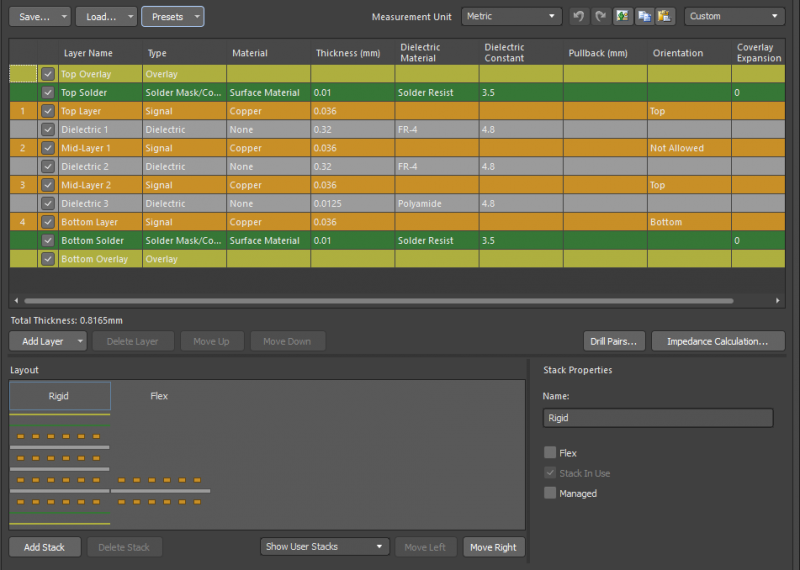
Planning a layer stack in flex and rigid PCB regions in Altium Designer
Mechanical Requirements for Flex and Rigid-flex PCBs
Working with a flexible printed circuit ribbon is all about ensuring components and traces on your board are not damaged under repeated bending. You’ll need to understand the mechanical properties of your materials to design the right bend radius, and many of the foundational concepts of rigid boards still apply. Although you want to prevent fracture, you also need to ensure your product will fit in its enclosure one the flexible ribbon is bent.
The ribbon in your rigid-flex and flexible circuit board will integrate directly into your layer stack as a signal layer and a pair of flexible surface layers. As you place additional features on a flexible printed circuit board, you’ll need to model your board’s mechanical behavior. This allows you to check component clearances and match your board’s dimensions to your board enclosure.
Flex PCB Bending Radius and Location
The bending location and radius need to be carefully placed during design so that the copper conductors do not fracture during deformation. For dynamic double-sided flex circuits, try to avoid laying traces over each other along the same direction.

Directly overlapping traces in a flex ribbon is not the best design choice.
Instead, traces should be offset to prevent excess stress concentration on the outer conductors during bending.

Offset conductors in a flex PCB ribbon.
If your flex circuit needs to carry a power or ground plane, you can use solid copper pours. However, you’ll have to accept significantly reduced flexibility and possible buckling if the bend radius is very tight. It’s best to use hatched polygons to retain flexibility. A normal hatched polygon still has heavily biased copper stresses in 0°, 90°, and 45° angle directions, due to alignment of hatch traces and ‘X’es. A more statistically optimal hatch pattern would be hexagonal. This could be done using a negative plane layer and an array of hexagonal anti-pads, but it’s fast enough to build the hatch below with cut-and-paste.
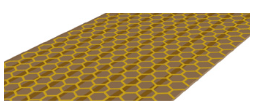
Hexagonal hatched polygons as a plane layer in a flex PCB ribbon.
The bending radius location is best placed along a straight section of conductors without any curve in the traces. The allowed bend radius can be calculated in terms of the allowed deformation on the outer edge of the copper conductors in the flex circuit. This is shown below.

Hexagonal hatched polygons as a plane layer in a flex PCB ribbon.
Thickness of the copper layer is specified in ounces per sq. in. For power and ground planes a 1 oz thickness of copper is usually used. For signal layers ½ oz copper is typical. Other copper foil thicknesses are available for specialized design. Once you define your bending radius, copper weight, and location in your polyimide ribbon, you can use some mechanical design tools to model how your board will bend and conform to its enclosure.
Working with Integrated ECAD/MCAD Tools
Working with integrated ECAD and MCAD tools in a single interface lets you do more than just verify clearances. You can directly design the enclosure around your finished circuit board layout by importing your design into popular mechanical tools. This is vital for ensuring your product complies with your mechanical requirements. It also allows you to simulate complicated flexible polyimide ribbon shapes.
- Designing all aspects of your rigid-flex board takes design tools with plenty of layout options. You’ll be able to design your polyimide flexible circuit zone, transition zone, and integration into your flexible or rigid-flex PCB stackup. Learn more about the layout features you need for flex and rigid-flex design.
- Your bending region is much easier to define when you have a 3D view of your circuit board. Working with MCAD and ECAD tools within a single program gives you a complete view of bending in your rigid-flex board, and allowing you to design the right packaging for your device. Learn more about working with integrated MCAD and ECAD design tools.
- When all these important rigid-flex PCB design tools are placed in a single application, it’s much easier to prepare your flex PCB prototype for manufacturing and generate deliverables. This includes Gerber files, assembly drawings, and much more. Learn more about preparing to manufacture rigid-flex PCBs and flexible circuits.
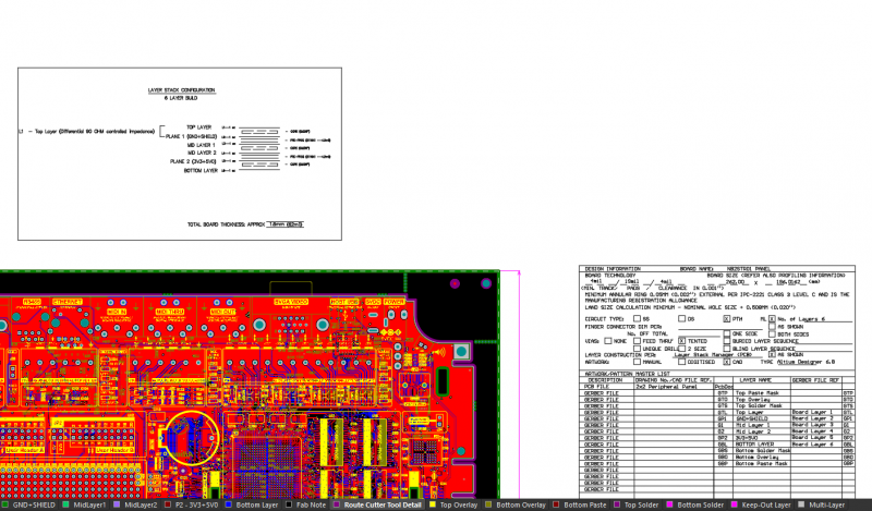
Port stackup information into your panelization and share in the assembly drawing
Flex and Rigid-flex PCB Design in Altium Designer
Some PCB design programs still force you to export a model of your board to an external tool in order to verify your bending clearances. Instead of working with external software, you can easily create a strong flex/rigid-flex stackup and layout, and you can verify mechanical constraints in a single program.
Altium Designer offers these important PCB design and layout features, and much more. You’ll have a complete toolset for rigid, rigid-flex, and flex circuit board design. The integrated ECAD and MCAD tools let you do more than just verify clearances. You’ll be able to design your board in three dimensions, offering much more detail compared to 2D tools for multilayer and rigid-flex PCB design.
Flex and Rigid-flex Design Starts with the Best PCB Design Software
Rigid-flex PCB design might seem like a complicated affair, but it doesn’t have to be when you use the right design tools. Design tools with integrated 3D design features, as well as standard routing and layout tools that operate in 3D, will easily adapt to rigid-flex and flex circuit boards. Altium Designer places all of these tools in a unified rules-driven design interface that is adaptable to any electronics application.
- Altium Designer’s unified design model integrates your design tools within a single software platform. You’ll have the flexibility to customize your devices, stackup, and components. Learn more about the unified platform in Altium Designer.
- Working with flex or rigid-flex PCBs requires customizing your layer stackup. Altium Designer makes it easy to customize your layer stackup. Learn more about best practices for layer stack design in Altium Designer.
- Working with multiple boards and rigid-flex designs is simple in Altium Designer. You can also define a flex ribbon to link multiple boards within the stackup manager, and the routing features let you easily route connections between each board section. Learn more about working with rigid-flex and multi-board design in Altium Designer.
Altium Designer’s Layer Stack Manager and Board Planning Mode are powerful features to get started with your layout. The routing features allow you to quickly define electrical connections between board sections, and the native MCAD features let you verify component placement and clearances. You’ll have everything required to design powerful rigid-flex and flex circuit boards when you use Altium Designer.
Altium Designer on Altium 365 delivers an unprecedented amount of integration to the electronics industry until now relegated to the world of software development, allowing designers to work from home and reach unprecedented levels of efficiency.
We have only scratched the surface of what is possible to do with Altium Designer on Altium 365. You can check the product page for a more in-depth feature description or one of the On-Demand Webinars.
