Complete Guide to PCB Design Reuse in the Cloud

Isaac Newton once said "If I have seen further it is by standing on the shoulders of Giants." Not all designs need to be remade from scratch, and if you organize your designs properly you can easily reuse your old design data in a new project. PCB design reuse practices are great for cutting down design time and ensuring all your products live up to the same level of quality. It’s all about making sure the knowledge you’ve gained from building great products can be adapted to new designs without constantly rebuilding the wheel.
PCB design tools already allow users to open old designs and start modifying them, but the best software platforms like Altium Designer allow you to enforce a structure to your old design documents that is ideal for PCB design reuse. If you’re working with a remote or on-premises design team, placing your old designs on the cloud is the easiest way to reuse old PCB designs in new projects while keeping your team productive.
When PCB Design Reuse is Right for You
Not every company will need to reuse all their PCB designs. Service bureaus that do a lot of one-off designs with fully custom engineering probably aren’t reusing their designs unless they are doing multiple revisions for a client. On the flip side, service bureaus that design a limited product range with standard form factors, common interfaces, or functional blocks may need to reuse designs when engaging with clients. Similarly, electronics companies might reuse portions of an old PCB design when developing a new product or upgrading an existing product.
There are a few portions of a design project that are prime candidates for PCB design reuse:
- Schematics: I’ve found this to be most common for my designs. We’ll create schematic sheets for different functional blocks in one design and we can build around these in a new design for a similar product.
- PCB layouts: If you change out a schematic, then you’ll need to change out components in the layout. However, there are functional blocks in a PCB layout that can be easily reused and replicated, for example, using rooms or snippets in Altium Designer.
- Components and libraries: This goes along with layouts/schematics as component data in a schematic or PCB layout needs to be carried into new designs. PCB design reuse can involve reusing specific components in any design, or reusing specific libraries in new projects.
- Templates: Design templates are a natural method for reusing design data. Templatizing a PCB layout or schematic drawing eliminates the need to redraw boards, logos, title blocks, or other features in your other design documents.
All of this is much easier when you store and share your design data through a managed cloud platform. Instead of using something like Google Drive or Dropbox, Altium Designer users can use the Altium 365 platform to easily store, share, and reuse their design data in new projects. There are a few critical features in Altium 365 that make PCB design reuse easy in these four areas:
Schematic Reuse
There are two easy ways to store, share, and reuse schematic sheets through the cloud:
- Within a project: When the entire project can be downloaded and opened in your PCB design software, you can grab schematic sheets and use them in a new design project. The new project can then be pushed back to your cloud environment.
- As individual schematic sheets: Individual schematic sheets can be downloaded from the cloud environment, copied into a new project folder, and imported into a new project.
Because Altium Designer integrates with the cloud environment in Altium 365, you don’t need to carry around library files. Altium Designer will bring the associated component symbols, footprints, and parameters into the new project automatically.
The image below shows how I’ve done this for an open motherboard project within my Altium 365 Workspace in my web browser. Note that I could also do this Altium Designer by just opening a managed project and copying the downloaded schematic file to a new project folder. I can also find my projects or individual files through the Open Project dialog in Altium Designer.

Schematics are a natural place to start with PCB design reuse as they don’t rely on any other design document. As long as you carry around the component library files, or as long as you’ve migrated components to your Altium 365 Workspace, you can easily reuse schematics in new projects. Simply download the schematic files from the Workspace to your local computer, and then drag these files into a new project in Altium Designer. Once you’ve gathered the important schematics and components for your new design, you can start determining if you want to reuse portions of a PCB layout.
Managed Schematic Sheets
Working with managed schematic sheets is a great way to create reusable circuit blocks for any design. These managed sheets can be downloaded from your Altium 365 web instance and added to a new project. These managed sheets store and track all data you would find in your schematic sheets in Altium Designer, including named ports, managed components, directives, and other data you’d find in schematic sheets.
PCB Layout Reuse
PCB layouts can be reused in the same way as schematics. Once the layout is imported into Altium Designer, you can copy and paste data between design documents. Whether you download a project or an individual PCB layout file, any reusable blocks in the layout can be pulled from the existing PCB layout file and into a new PCB layout. The image below shows how you can take advantage of Rooms in a PCB layout to copy groups of components between PCB layout documents.
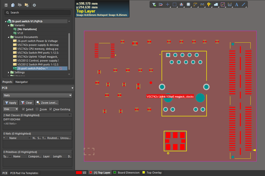
The easiest way to do this is to open your managed project in Altium Designer, and then copy portions of the layout into a new PCB layout document using the regular copy and paste features. Make sure the destination PCB is attached to a new project, and make sure the copied circuit block has its corresponding schematics attached to the new project. Once the circuit block is copied to the new project, it’s best to run an “Import Changes To…” command to ensure that no components in the destination layout were missed. Any missed components will be pulled from the schematic sheet into the new PCB layout document.
Library Migration and Component Reuse
Components and libraries are natural candidates for reuse, and it’s common to provide custom libraries to a design team when proprietary parts are used in a design. When old components are present on a managed cloud platform that integrates with your design tools, you can place components from one design into any other design. One way to do this in Altium Designer is to use the Library Migration feature. This will put select components in your design libraries into the managed cloud environment in Altium 365, and they can be imported into your designs through the Explorer Panel.
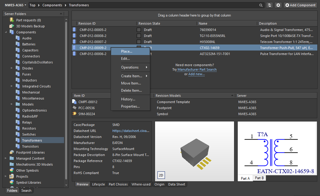
Within Altium 365, you can even reuse existing footprints and schematic symbols for new components. This is useful when working with proprietary components, connectors, printed waveguides or antennas, or any other component that comes in a common package. This is a much faster way to create a new component than copying and pasting schematic symbols between libraries.
To do this, follow this link to learn about using the library migration tool in Altium Designer so that you can bring your libraries into your Altium 365 Workspace. Once your libraries have been migrated over to your Altium 365 Workspace, you can access individual footprints and schematics within Altium Designer. You can now create a new component and begin adding the following information to your component:
- Schematic symbols: Select the “Existing” option from the symbols entry and look through the Symbols Library in the Explorer dialog. Select the existing symbol you want to use for the component.
- PCB footprint: Here, you’ll look through the Footprints Library entry in the Explorer dialog.
- Simulation model: This isn’t mandatory, but it is useful if you want to use the component in SPICE simulations in the Schematic Editor.
- Parameters: This is where you can fill in any of the typically required information for sourcing (manufacturer, MPN, supplier information, etc.), electrical parameters, and a description for the components.
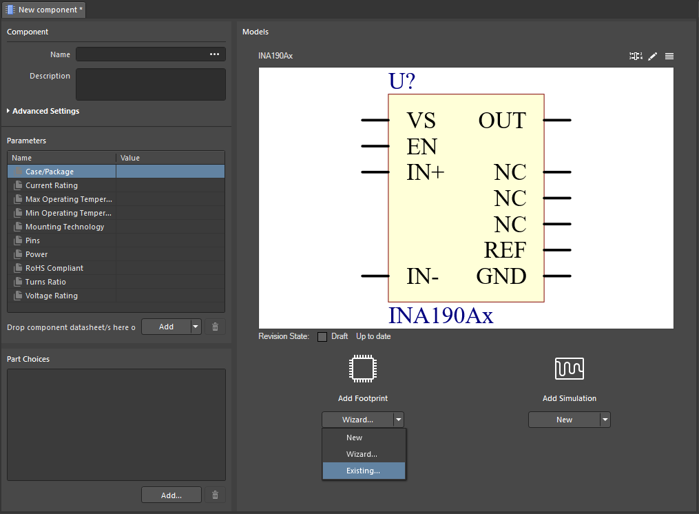
This is a great way to create a new component that has a standard package (e.g., QFN, SOT, etc.), or to reuse an existing symbol for a component but in a new package. Always make sure to validate your new component against the datasheet to be sure there are no footprint or symbol errors.
Templates
Schematic and PCB layout templates are probably the most common way to reuse PCB design data, but Altium 365 does more than let you reuse these two types of files. Components, projects, PCB layer stacks, bills of materials, and manufacturing outputs can also be templatized and quickly reused in a new project. The image below shows how you can access component templates through the Altium 365 web instance. These templates can also be downloaded to a local machine or accessed within Altium Designer.
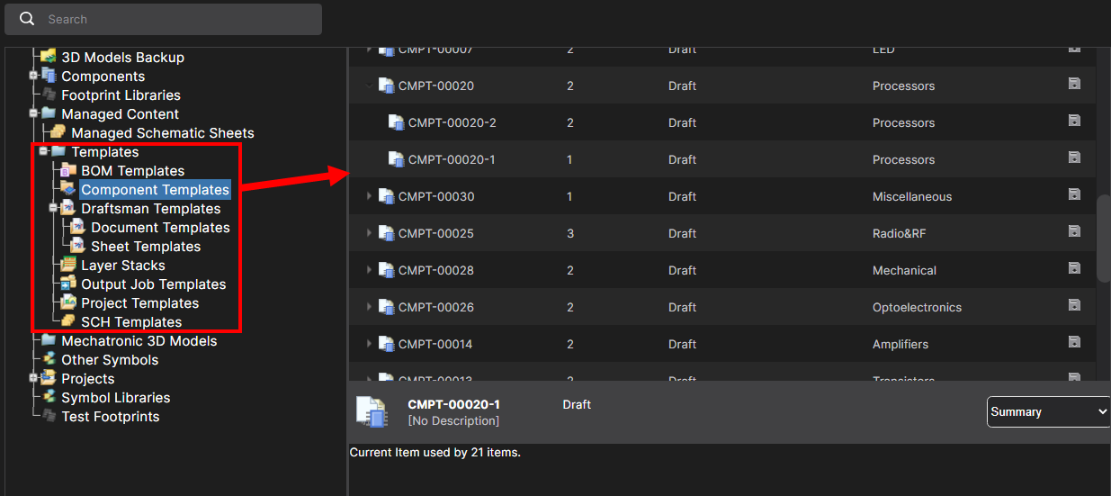
In the above image, you’ve probably also noticed the entry for Output Job Templates. This is a convenient way to save settings for manufacturing files. If you work with a small number of manufacturers and each has particular requirements for project documentation, some design programs let you customize your output configuration so that you won’t have to set up a new configuration for each project.
Why You Should Use Altium 365 for PCB Design Reuse
Altium 365 is the only managed cloud platform for storing and sharing PCB design projects, and it makes PCB design reuse easy. This platform integrates with Altium Designer, and design teams can quickly use old design data to start building up a new project. In addition to PCB design reuse, Altium 365 users have access to other features and benefits that today’s PCB design teams need:
- Organization: Altium 365 enforces a simplified organization for storing project data, component data, libraries, and much more on a managed cloud platform.
- Simple, secure access: A designer can easily share a project with another designer, customer, or other stakeholder, and they can access the project through a secure web interface or through Altium Designer. Different users in an organization can be given different levels of access to a project.
- Put a design into manufacturing: You can quickly share your design with your manufacturing team and invite them to collaborate on a thorough design review.
- Convenience: Best of all, designs can be accessed from anywhere. As long as you have an internet connection, you can pull your design data into Altium Designer and start working on projects.
Today’s PCB manufacturers and PCB designers can use the Altium 365™ platform for all these points and more. PCB design reuse, PCB design reviews, and pushing designs into fabrication are all easy with Altium 365. This unique cloud-based platform integrates with the world-class design tools in Altium Designer®, making all your project data accessible to your manufacturer and collaborators in a secure environment. Designers and manufacturers can share PCB fabrication data, project files, and much more in a cloud-based platform.
We have only scratched the surface of what is possible to do with Altium Designer on Altium 365. You can check the product page for a more in-depth feature description or one of the On-Demand Webinars.
