Class-D Amplifier Design and PCB Layout

Amplifiers can come in all shapes and sizes, depending on their bandwidth, power consumption, and many other factors. A Class-D amplifier design is normally used with high fidelity audio systems, and circuits for a Class-D amplifier are not too difficult to build in a schematic. If you’ve never worked with a Class-D amplifier or you’re looking for a fun audio project, follow along with this PCB layout.
A Simple Class-D Amplifier Design Prototype
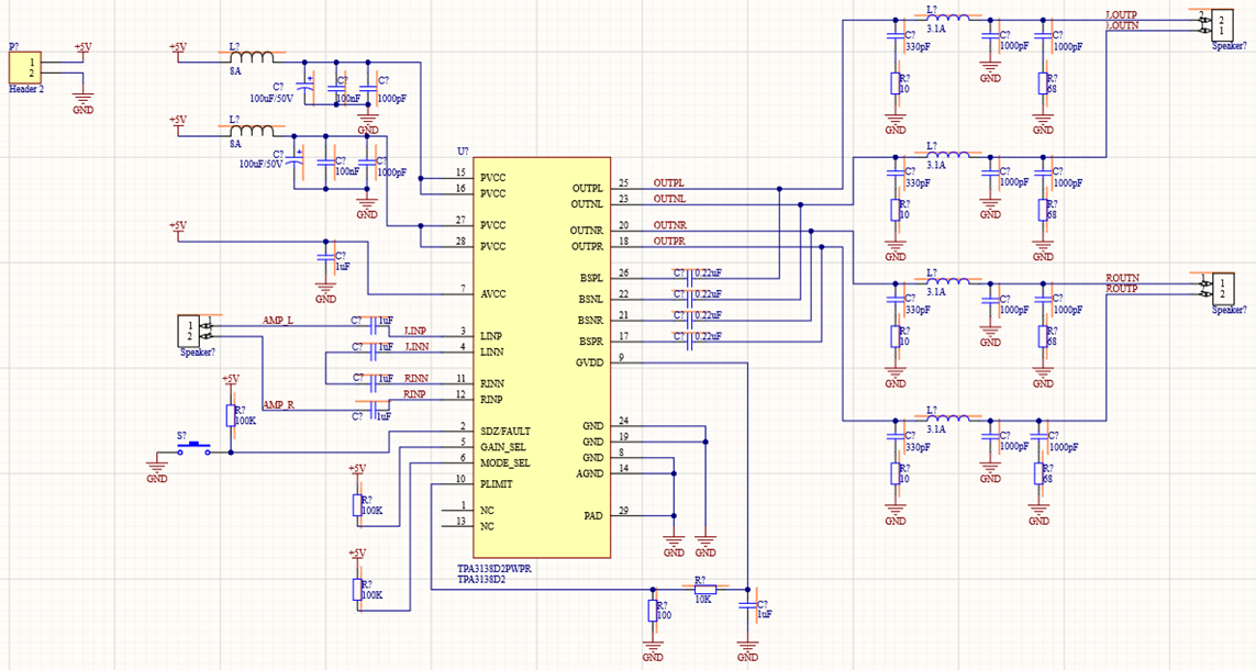
The board I’ll present here is more complicated in the schematic than in the layout, but it is something you could create from another proven design. The central component in this board is the inductor-free TPA3138D2 Class-D audio amplifier. The layout I’ll show is similar to the breakout module for this component, but some differences will help ensure noise suppression and EMC. In addition, the banana clip jacks on the breakout board have been replaced with standard 3.5 mm audio jacks.
Schematic
This schematic has a lot of components clustered around a single IC, as shown in Figure 1 below. In this type of arrangement, it’s okay to wait until the schematic is finished before assigning reference designators; thus, there are the red error bars beneath components in the schematic. Just ignore these, for now, they’ll disappear after you assign unique designators.
Part Selection
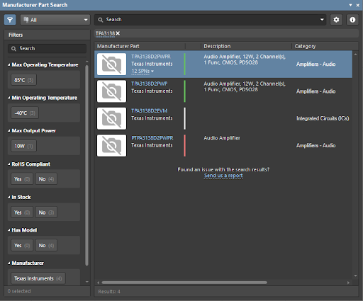
Aside from the main TPA3138D2 Stereo Class-D Speaker Amplifier, there aren’t many special steps that need to be performed before we can proceed to the PCB layout. The first thing we need to do is grab the TPA3138D2 component from the Manufacturer Part Search panel. From here, we can place it directly in the blank schematic and start adding other passives in the device.
Other passives should be chosen to handle appropriate power output (resistors) and voltage with appropriate capacitance. Since we aren’t worrying about very high frequencies in this amplifier, we can use electrolytic capacitors.
Designators
As far as assigning designators, you should try to keep them organized, especially if you will be using multiple sheets in your project. I would start assigning reference designators in the upper left corner of the schematic and work my way diagonally across the sheet. You could also replace the connectors with some ports pointing to other sheets if you want to use this circuit within a more extensive system.
Differential Output
If you look closely in the schematic, you’ll notice that the left and right outputs are differential pairs. Here, I could place a differential pair directive if we needed to apply a large number of design rules to multiple differential signals. I’ve left this out here as we are not worried about impedance controlled routing. We only need to ensure length matching for these signals, which is easy enough to do in the PCB layout.
Power
You’ll note here that I haven’t placed power regulation on this board. Still, you could certainly add a power regulator to the schematics as long as it can supply up to the 18.5 W maximum output power as specified in the TPA3138D2 datasheet. You could add a simple power regulator unit in a different schematic and import this into the board to provide 5 V power. On this board, I’ll add power through a pin header to keep things simple.
PCB Layout
Although the schematic looks a bit crowded, the major component that needs to be placed and routed carefully is the TPA3138D2, as well as the traces routed out to our input/output connectors. Before getting started with the layout, there are some important EMC rules that we would want to obey in order to prevent low-level noise from being output to the speakers connected to this board.
Since we’re not dealing with extremely high speeds (only up to ~1 MHz bandwidth for slow PWM signals), we should follow some standard PI, EMI, and EMC guidelines when planning the PCB layout.
- Power: Use a continuous ground plane on an internal layer, and keep planes away from the edges of the PC board. For this board, you could use a power plane, but we aren’t running at very high current, so it’s not necessary. Instead, I’ll use some thick traces for routing power from the power header to the components and for routing from the amplifier output to the speaker connectors.
- Routing: Keep amplifier output traces to the speaker as short as possible. These traces and the speaker wires will be the largest sources of radiated EMI.
- Caps: In this type of low-speed design, the normal recommendation is to use 1 nF low-ESR caps near the TPA3138D2 IC to damp ground bounce and minimize parasitic inductance. There are two large capacitors (0.1 mF/50 V) on the input to the PVCC pins in the upper left portion of the TPA3138D2 chip (see Figure 1). Radial capacitors can be used so that they take up small board space. For mid-frequency noise due to the PWM signal and its transients, you can also use a 0.1 µF capacitor placed as close as possible to the PVCC leads.
- Parasitics: Here, we’re mostly worried about keeping loop inductances small for critical traces. This is another reason to use a continuous ground and place the speaker output close to the amplifier.
- Heat sink: At 4 or 8 Ohms (standard speaker impedance), and the rated power output, you would want to have a thermal strategy in place. Having the ground plane beneath the module helps, but the TPA3138D2 is large enough that a small heat sink could be placed on it.
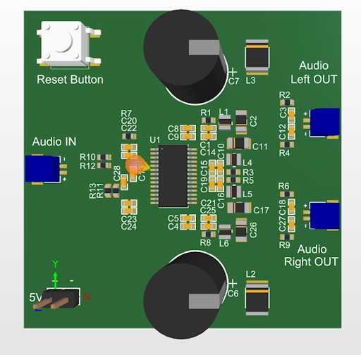
Figure 3 below shows the finished layout in 3D (access this by pressing “3” on your keyboard with the PCB editor open). The strategy I’ve used is to place the output connectors by the edge of the board and work backwards to the power port. After placing the output connectors, I placed the TPA3138D2 amplifier, routed traces between the amp and speaker outputs, and placed the remaining passives around them. Finally, I kept the power connection in the lower left side region of the board. If you wanted to include an onboard switching regulator, this would be a good spot for it as it’s far away from the audio output traces.
In Figure 4, you’ll find the 2D PCB layout. This board was designed on two layers and included multiple polygons to provide power to the amplifier section. In this board, it’s easiest to route the thick traces to the speaker outputs using polygon pour. The bottom layer contains a solid ground plane, and there are multiple via fences placed in the layout to provide a bit of isolation between the left and right sides of the board. You’ll notice that the top layer has also been filled with the ground to provide shielding for the input audio signals.
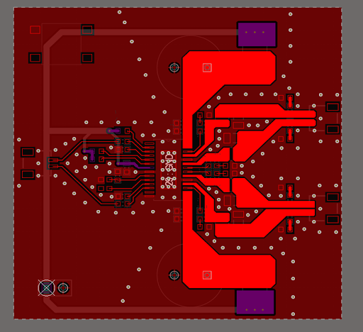
One point to note is the large copper fill regions leading to the output connectors. These traces are a bit overkill for this board, but the board will carry high power, so it’s okay to opt for bulkier traces to help keep the temperature low. In contrast, the traces on the input side are much smaller as we’re assuming the input signal will be a rather low level.
If you’re happy with your Class-D amplifier design and layout, you can use the manufacturing features in Altium Designer® to get your board ready for fabrication and assembly. You could also share your new board with your collaborators or manufacturer on Altium 365®. We have only scratched the surface of what is possible to do with Altium Designer on Altium 365. You can check the product page for a more in-depth feature description or one of the On-Demand Webinars.