Wideband Signal Analysis in Ultra-high Speed PCB Design

Many design guidelines, which were perfectly applicable 10-20 years ago, hold to the same mantra around high speed signals: pick a single frequency to use for you calculations, and design to that frequency. For lower edge rates, this was usually fine because deviations from typical low-frequency values simply aren’t noticed. Modern computer interfaces and common high speed signaling standards used in embedded systems require a better approach than simply using a single limiting frequency.
When working on a high speed design, a good design and analysis approach should account for the entire bandwidth of the signal in question, not just a single limiting frequency. Analog signals are simpler because their bandwidth is smaller, but circuits for analog components still need to have flat response throughout the bandwidth to prevent signal degradation.
What is a Wideband Signal?
Like many engineering terms, the word “wideband” is a relative term; one engineer’s wideband signal is a very narrowband signal. In general, a wideband signal is a digital or analog signal that contains frequency components spread out over a broad range. The range over which frequency components are spread could be a few percent of the carrier frequency (e.g., a typical FM signal), or it could span many octaves (e.g., a truncated digital signal). In any case, we are designing a board or analyzing a measurement that is prominent over a broad range of frequencies.
Consider NRZ and PAM4 signaling. These two signaling schemes are decidedly wideband; the Nyquist frequency of each is 1/2 and 1/4 the baud rate, respectively, but distortion and errors can be seen beyond 5x the Nyquist frequency. Clearly, what happens at such high frequencies matters, but older design methods tell designers to just consider what happens at one frequency.
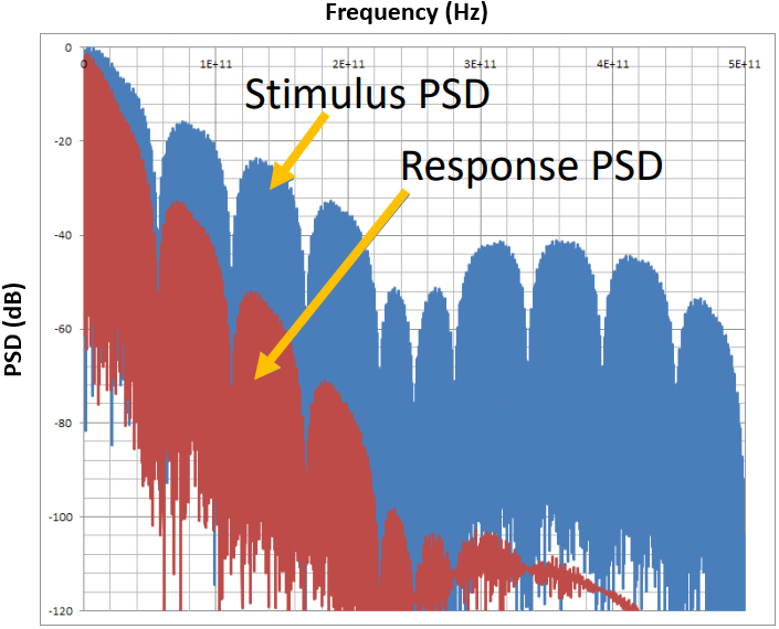
When a typical high speed signal is spread across a huge range of frequencies, which frequency do you use to design your interconnects? The example image below from Heyfitch and Shlepnev shows that the answer is not so clear.

The image above should be instructive and inform you why working throughout your signal bandwidth is so important. The blue graph shows the power spectral density of a PAM4 pseudorandom binary bit sequence with 4 ps edge rate, and the red curve shows the response measured at the Rx end of an interconnect (only 25 cm trace on a PCB). Losses occur primarily at high-GHz frequencies that would normally be associated with mmWave signals. The truth is, more digital designers will need to work at these frequencies to accommodate faster edge/baud rates in high speed signaling standards.
Getting Started with Wideband Signal Analysis
First things first, wideband signal analysis starts in the frequency domain (see the above PSD plots!) as this is the only way to see the signal’s bandwidth and how your PCB responds at different frequencies. In PCB design, wideband signal analysis can be used to evaluate signal integrity metrics across the signal bandwidth, rather than just at a single frequency. This is the analysis approach taken in the USB 4.0 standards, and I take the same approach in other areas.
There is no fixed process to follow in wideband signal analysis. Instead, you need to think about the important signal integrity metrics that matter for your design. In some cases (e.g., USB 4.0 standards as I mentioned above), a wideband metric may be specified, which you can then use for comparison. During design, you’ll need to rely on your signal integrity simulation tools to examine wideband signal behavior.
Here’s the general process for examining wideband signal behavior in different designs:
- Choose a phenomenon that matters in your design. Examples include crosstalk between critical nets, signal distortion (calculated from a transfer function), insertion loss, return loss, and power bus ripple/ground bounce (on the PDN). Some upper/lower limit needs to be imposed to ensure your design functions properly.
- Simulate the relevant phenomenon and convert to the frequency domain. Taking a Fourier transform puts your data in the frequency domain, which will then be used to quantify whether you’ve met your design goal.
- Formulate a figure of merit for your design. When doing wideband signal analysis, you need to have some metric that quantifies whether you’ve met your design goal throughout the signal bandwidth. This is normally formulated as some integral in the frequency domain, which is simple enough to calculate numerically.
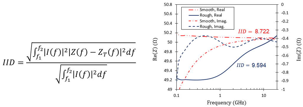
To illustrate Point 3, the example below comes from my own work designing striplines for a high speed board. I’ve given this figure of merit the name “integrated impedance deviation” (IID) in an effort to follow the same track as others who work with broadband design metrics in SI-aware designs. This naming scheme is similar to what is used in USB 4.0 (integrated differential crosstalk and integrated return loss), except this particular metric is a comparison rather than a calculation of a specific metric.
Example: Integrated Impedance Deviation
When trying to design a transmission line to a target characteristic impedance, dispersion in the substrate and roughness in the copper trace will create odd deviations from the target impedance within the frequency domain. The magnitude of IID throughout the design bandwidth tells me how well I’ve met the impedance requirement for my design. In the definition below, ZT(f) is my target impedance, and Z(f) is an impedance determined from analytical models, simulations, or numerical models. The spectrum I(f) is the input current spectrum, which is used as a weighting function in this definition. This essentially lets us state which portions of the signal bandwidth are most important for impedance matching.

In the above graph, we can see that the IID values for our rough and smooth lines are very similar given this input current pulse, even though their impedance spectra are quite different. This can be explained by the magnitude on the left y-axis (real part of the impedance); the scale here only spans ~2 Ohms, and the range of imaginary values is quite small in comparison (only ~2%). Both lines are very well matched considering the addition of roughness in the design; in fact, there is only a 2% difference in the trace width-to-height ratio for these lines.
The other important point to note above is that this comparison is valid for a specific input pulse. Therefore, if we want to examine a different input pulse, we would have a different IID value for that channel. These types of comparisons can even apply to inherently bandlimited signals (e.g., frequency-modulated signals), which would then account for the limited relevant bandwidth and the portion of the signal that contains the most power.
Using Wideband Signal Integrity Metrics
If you’re determining wideband signal analysis metrics for your own class of designs, or you just need to examine deviation from a target value over a broad bandwidth, you’ll find the above formulation useful. The equation above is basically the root-mean-square error between the voltage of a broadband signal on my designed stripline and the desired signal on the stripline. This difference arises due to a difference between the design impedance Z and the target impedance ZT.
Here, the design goal would be to adjust the signal geometry such that IID remains below some acceptable level. If IID is too large, then the difference between the design and target impedances is too large. Similar approaches can be taken with other signal integrity metrics (e.g., crosstalk, losses, phase response flatness, etc.).
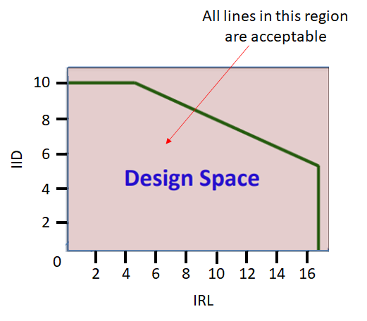
One strategy is to use wideband signal integrity metrics to develop a “design space”, a term that is related to the feasible space as defined in optimization problems. The idea here is to use the relevant signal integrity metrics you’ve deemed important for your design to determine an acceptable range of possible metrics that satisfy your design requirements. This takes a lot of work on the front-end with simulations, such as field solver calculations or IBIS simulations, but it will help you develop a set of acceptable limits on signal integrity metrics in your design.

By definition from optimization problems, the design space you develop could be a very complex multidimensional graph that cannot be easily visualized. The simplest design space that tries to balance two metrics is a 2D space, as shown in the example above. In this example, I’ve plotted acceptable limits on IID and integrated return loss (IRL) as defined in USB 4.0. While you can develop these design spaces using simulations, the best strategy is to account for signal integrity using measurements.
Working with Measurements Instead of Simulations
Some quantities, such as periodic loading due to fiber weave effects, cannot be easily simulated with EDA tools. In this case, you can still calculate integrated wideband signal metrics to quantify signal behavior, but you’ll use your measurements instead of simulations. Here, you would want to calculate the figure of merit from your data, and then compare it with your design goal.
When you use Altium Designer®, you’ll have the signal integrity simulation features you need for wideband signal analysis. You’ll also have a complete set of CAD tools to create and modify your PCB design. Altium Designer on Altium 365 delivers an unprecedented amount of integration to the electronics industry until now relegated to the world of software development, allowing designers to work from home and reach unprecedented levels of efficiency.
We have only scratched the surface of what is possible to do with Altium Designer on Altium 365. You can check the product page for a more in-depth feature description or one of the On-Demand Webinars.
