Taking a Modular PCB Design Approach in Altium Designer
PCB design is rarely discussed in terms of designing to functional blocks or as connecting modules with different functionality. Simple designs can usually be designed without considering how your PCB layout affects the operation and interaction between multiple functional blocks in your board. With more complex designs, you’ll need to consider more than just the high-level overview of your board when you are designing a complex system.
Modular PCB design is one design methodology that is implicitly used when designing PCBs for a variety of applications. Embedded systems, multi-board systems, mixed-signal systems, and other boards with diverse functionality can all benefit from this design methodology. New designers would do well to learn anything they can about modular PCB design.
When you take your first dive into modular PCB design, you’ll quickly find that your design tools may not be able to keep up due to a lack of unification, inconsistent data formats across design tools, and unnecessary repetition of basic design steps in different tools. Design software is finally catching up to the demands of modular design, and PCB designers can finally access design platforms packages that are uniquely adaptable to modular PCB design.
ALTIUM DESIGNER®
A unified PCB design package with the most adaptable set of design tools in the industry.
In the past, PCB design treated each portion of an overall electronic system individually. The links between different portions of the system were seldom considered except by designers creating the most complex boards. Some examples include computer architecture and peripherals, embedded systems for military and aerospace, and other complex multi-board systems.
Now that electronics in all sectors of the market are becoming smarter and connected, consumers are demanding greater functionality from electronic products. PCB designers need to think in new ways in order to integrate all this functionality in a single device. Modular PCB design is one design approach that takes a hierarchical view of an electronic system, whether it be a rigid-flex, multi-board, mixed-signal, or other system.
Design software that operates with a consistent, unified interface and a single data model is uniquely capable of being adapted to modular PCB design. This allows you to define a rigorous hierarchy for your system and quickly implement it in your next device. With this in mind, let’s take a look at the modular PCB design process and how you can take a hierarchical approach to designing complex systems.
The Modular PCB Design Process
Thinking about modular design requires looking at your device in terms of its separate functionality. This is by far the easiest when you start with a functional block diagram of your device. You want to start with a high-level view of how different portions of your device work together to produce the key features you need. You’ll need to consider inputs and the desired outputs in your functional block diagram.
In cases where your device will contain some central processing, you’ll need to consider this as part of the overall design process. This is about more than just creating a block diagram; you may need to make changes to your design later when you start laying out your board if you do not consider this early. Many designers will start immediately laying out their board around some central component without thinking about the relationships between functional blocks in the system.
Once you are ready to drill down to a more granular level of your board’s functionality, you may want to create finer block diagrams that show how each portion of your device functions. In other words, you want to take a hierarchical approach to designing your board’s key features.
Using Schematics for Modular Design
Creating schematics is your first step to taking your board off the back of a napkin and into your design software. When it comes to modular design, you can get a head start on schematic design when you design connections between components within each functional block in your block diagram. This gives you a head start on designing each PCB schematic and gives you a useful reference once you start designing each circuit.
Schematics can be linked together using a hierarchical schematic editor that is uniquely tailored to printed circuit design. This allows you to define parent-child relationships between multiple schematics. This also helps you stay organized throughout the design process and allows you to remain focused on one portion of your design at a time. You can then link multiple schematics together within a higher level parent schematic, similar to the way you would in a functional block diagram.

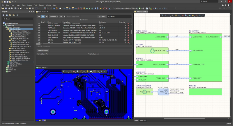
Hierarchical, multi-board design for printed circuit layout
In many systems, you will reuse certain portions of your design, and there is no reason to continually redesign portions of your board in different schematics. This is where multichannel design becomes critical. This design methodology allows you to easily reuse portions of your design in different schematics. You won’t have to re-add and rearrange the same components multiple times in your schematics.
Once you have defined parent-child relationships between schematics and completely translated your functional block diagram into a set of hierarchical schematics, it’s time to transition to the PCB layout phase. You’ll need to capture your schematics as initial layouts on a new board with a schematic capture tool. Once you have captured your components and connections on an initial board, it’s time to start arranging and routing components.
If you’re creating a multi-board system, this design process is naturally adaptable to multi-board design. Each functional block or multiple functional blocks can be integrated into different boards, making schematic capture to each board much easier.
- The modular PCB design process is much easier when your schematics help you stay synchronized with each other and with your PCB layout. Hierarchical schematics help you stay uniquely organized throughout the design process.
- The right design software with a unified set of tools will help you adapt your process to modular PCB design.Learn more about the modular PCB design process.
- The right PCB design software will naturally integrate your schematic data, layout, and component information using a single data model. This naturally aids the modular PCB design process.See how integrating schematics, layouts, and databases aid modular design.

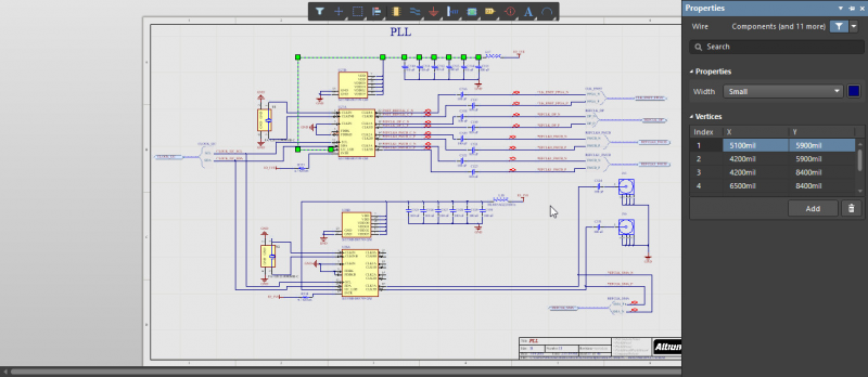
Schematic design as part of the modular PCB design process
Modular PCB Design: The Layout Phase
Once you capture your schematics as an initial layout, it’s time to start arranging components around your board. The right schematic capture tool will maintain the organization you defined in your schematic and will show you the connections between components as part of your schematic.
Some boards will need to have functionality that is separated into different portions of your board or literally onto different boards in the case of a multi-board system. For example, mixed-signal systems should be designed so that the digital and analog sections form their own functional blocks, and each block will need to be separated into its own areas in the board to preserve signal integrity.
Once you add even more functionality, such as a Wi-Fi module for wireless communication, it should also sit in its own functional block and may even need its own schematic. You’ll want to assign each type of functionality to its own area of your board to preserve signal integrity and ensure that your device operates as intended.
In the realm of computer architecture, for example, multi-board systems separate important functionality into different blocks in order to provide different functions while meeting specific industry standards on design and functionality. This is just one area where a modular design approach is indispensable.
Modular PCB Design Software
PCB design software for modular design requires a number of functions that other design platforms simply can’t offer. Your modular design software needs to include hierarchical, multi-channel schematic editing tools to separate the key features of your system into functional blocks. You’ll operate at your highest productivity when your design software includes a schematic capture tool alongside your schematic editor.
Component management is another important part of modular PCB design. When working with multichannel design, you’ll be reusing plenty of components in different locations throughout your board. This means you’ll need a component library that integrates with all of your design features using a unified component data model.
Integrating these features into a single interface allows you to easily generate initial layouts and start arranging components throughout your system. Your layout editor should also allow you to group components into groups in your layout, making it easy to rearrange components in your system as needed. This helps you stay organized and correct layout errors before you move on to manufacturing.
- Modular design is a natural multi-board design methodology. Separating functionality onto different boards is a natural way to ensure your system stays organized and works as intended.
Learn more about multi-board design with PCB expert Ben Jordan.
- Modular hardware for IoT devices can be easily integrated into a complex multi-board system when you use modular PCB design software.Learn more about working with modular IoT modules.
- Any manufacturer will need a complete documentation package for your board. Working with integrated design software makes modular PCB design much easier and allows you to quickly generate documentation for your manufacturer.
Learn more about creating documentation for your manufacturer.

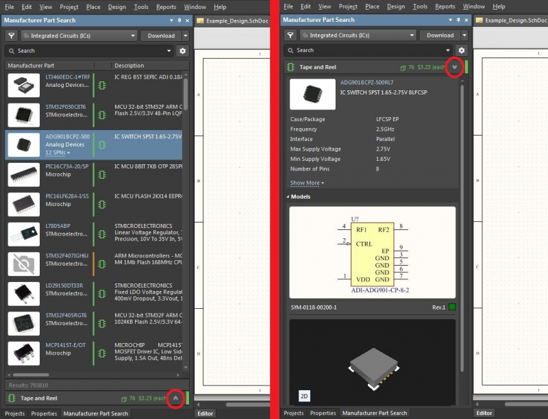
Component manufacturer search tools integrated with your schematic editor in Altium Designer
Software-aided Modular PCB Design Applications
There are plenty of applications that can inspire your next design and will benefit from a modular design approach. Computer architecture is one area that has long used a modular design approach, albeit across different companies throughout the industry. With more consumer-level products including sophisticated functionality and providing connectivity, taking a modular approach with the right design software will help you successfully design for these applications.
Products like wearable medical devices, smartphones, entertainment systems, home automation systems, and connected automobiles are embedded systems that naturally apply a modular design approach. Many devices in these areas are actually multi-board systems that require sophisticated design tools to help you create a functional design and prepare it for delivery to your PCB manufacturer.
While modular design software includes broad functionality, it doesn’t need to make the modular design process complicated. When these tools are integrated into a single program, the modular design process will be much easier and can proceed quickly. Instead of separating tools into separate programs like other PCB design software companies, your design software should contain the tools you need to create comprehensive systems using any design methodology, including modular design.
Modular Design in a Unified Environment
Working in an environment that unifies your design features gives you access to more than just sophisticated schematic and layout editing tools. The integrated design environment in Altium Designer operates using a single rules-driven design engine and a single data model for your components and board. This allows features like simulators, data management, and documentation tools to instantly access your design data as you prepare for manufacturing.
Simulation is an important part of modular design as you’ll need to verify important aspects of your power distribution network, crosstalk, and EMI suppression. Working with an integrated design platform allows your design data to be passed directly to your simulation tools. You won’t have to export your design to another program. This also allows you to limit your simulations to specific functional blocks within your system.
Working with a rules-driven design ensures that your design features will instantly check your schematic and layout choices against your design rules. As part of modular design, you’ll need to make sure that each functional block in your design will operate as expected and that it meets basic design standards.

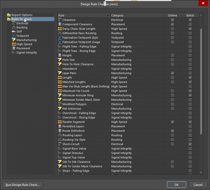
Interactive design rules checking in Altium Designer
Altium Designer is the only design software that integrates all these features and more into a single, unified design environment governed by a rules-driven design engine. This ensures your tools are naturally adaptable to modular PCB design and integrates these tools into a single design environment. You’ll have the power you need to design to any application with Altium Designer.
- The multichannel, hierarchical schematic editing tools in Altium Designer are a natural choice for modular PCB design. These features allow you to quickly capture your schematics without switching to a separate program.Learn more about hierarchical, multichannel schematic design in Altium Designer.
- The rules-driven design engine checks all aspects of your schematics as part of modular design. This also allows your design features to naturally communicate with each other in a single data format.Learn more about rules checking for modular design in Altium Designer.
- When it’s time to send your board off for production, the design tools in Altium Designer easily integrate with your documentation and sourcing features. You can quickly generate the documentation you need and bills of materials for your board.Learn more about bill of material management in Altium Designer.
Modular PCB design requires visualizing your designs in a new way, and your PCB design software needs to keep pace with new design methodologies. Altium Designer is the only software package that is uniquely adaptable to any design technique and application. Once you use Altium Designer, it will be the last PCB design software package you’ll ever need, and you’ll have the tools you need to stay at the forefront of new technology.
Using the integrated design interface in Altium Designer for modular PCB design might seem daunting, but Altium offers plenty of resources to help you reach success. With instant access to the AltiumLive forum, podcasts, and webinars given by industry experts, design tutorials, and an extensive knowledge base, you can rest assured you have the tools you need for any design. No other PCB design software company gives you access to this many resources.
Only Altium Designer places all the design, simulation, verification, and documentation tools you need into a single program with a consistent interface. Instead of using an outdated workflow in other design software platforms, try working in the only design environment that is uniquely adaptable to any design methodology. You can stay at the forefront of modular PCB design when you use Altium Designer.
