Smart Micro Fan Controller
If you’ve ever had to wear eye protection for an extended period of time, especially if you have prescription inserts in that eye protection, you’ve probably noticed fogging can be a major issue. Last year I designed and 3D printed a small fan unit that mounts a 25mm x 25mm x 10mm fan on each side of a military eye protection. It directs a small flow of air over the inside of the lenses and keeps them clear even during physical exertion on cool humid days, allowing the wearer to maintain clear vision. It uses a small 2 cell lithium polymer battery mounted on the back of the eyewear’s band, which feeds the 12 fan - it’s enough to keep the fan spinning but uses very little current and is not audible despite the fans being right next to your ear. There are some issues with this system however, firstly there’s no battery protection, so during extended periods of use the battery can be completely depleted beyond the point it can be recharged safely. Secondly, there’s no speed control, so you’re stuck with the airflow speed the battery provides, which is generally fine but occasionally a small burst of extra airflow would be useful.
On the surface, it is a relatively simple project to design a device to operate as a fan controller, but the application and design requirements add some interesting constraints. The project had the following constraints to take into consideration:
- PCB dimensions should be 25 mm x 10 mm
- Components should be placed on one side of the PCB only
- PCB should ideally be 2 layers but could be 4 layers if necessary
- The device must be able to control a small 5V fan
- The device will be powered using a small single cell Lithium Polymer battery
- There should be no Ball Grid Array (BGA) package components on the PCB
- Battery connector placement must be as specified
The fan controller needs to have the following functions:
- The fan speed should be controlled by a microcontroller using PWM
- The user should have the ability to turn the device on and off and select different fan speed modes
- The device should have a battery charge indicator in the form of an RGB LED.
- Hard switch off when battery voltage is critical.
The PCB size is determined by the fan, I want to have a circuit board that can sit on one edge of the fan so as to be as compact as possible. This also drives the requirement for single sided components, and impact/shock as well as hand assembly leads to my no BGA packages. For a board this size, anything BGA is likely to be wafer scale, and therefore extremely fine pitched which can be more challenging to hand place than the wider pitched BGA packages commonly found in larger packages.
To switch the device off when the battery voltage drops too low, I’ll be implementing a “Suicide Switch”. To turn on the device, the user will press the one button on the device which will pull the regulator’s enable pin high, allowing the microcontroller to boot and assert that pin high itself. Once the microcontroller determines the battery voltage is too low, it can pull the voltage regulator enable pin low, switching off the unit and ceasing any current draw. For this type of device, it’s a more optimal solution than simply putting the microcontroller to sleep, as if the unit is in storage it could damage the battery through over-depletion from the micro-current draw.
Component selection
Compared to the previous design, I wanted each fan unit to have it’s own battery that can be quickly swapped. The radio controlled model industry has some fantastic options for small batteries, which lead me to using a 150mAh battery that is common in small indoor helicopters and planes - they are extremely cheap, high quality and have tremendous discharge capabilities. This size battery is relatively well standardised, so the board will use a Molex Picoblade (Molex51021-2P) connector for the battery. For placement, the battery should be at the top of the board/fan unit, which will make placing a small button at the bottom of the board accessible while the unit is mounted on the wearer’s eye protection. This will also place the fan along the glasses arm in the final assembly, which keeps things nice and compact.
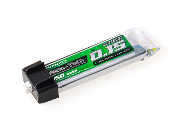
https://hobbyking.com/en_us/turnigy-nano-tech-150mah-1s-25-40c-lipo-pack.html?___store=en_us
The battery's electrical parameters and mechanical dimensions are as follows:
Capacity: 150 mAh
Voltage: 1 cell / 3.7 V
Discharge: 25C Constant
Weight: 5 g
Dimensions: 40 mm x 12 mm x 5.5 mm
Balance Plug: Pico (Molex51021-2P)
Discharge Plug: Pico (Molex51021-2P)
Where the original design used a 12V fan, that is not a particularly practical choice for a design powered by a single lithium polymer cell. For the new design, I’m using a 5V variant in the same 25x25x10mm size.
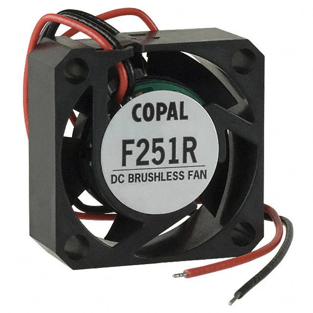
https://www.digikey.com/product-detail/en/nidec-copal-electronics/F251R-05LB/563-1109-ND/1165503
The fan's electrical parameters and mechanical dimensions are as follows:
Voltage - Rated: 4.2 ~ 5.7 V
Current Rating (Amps): 60 mA
Size / Dimension: Square - 25 mm x 25 mm
Width: 10 mm
Weight: 0.015 lb (6.8 g)
Air Flow: 1.8 CFM (0.050 m³/min)
Power (Watts): 300 mW
RPM: 8000 RPM
Generated noise: 15.0 dB(A)
Termination: 2 Wire Leads
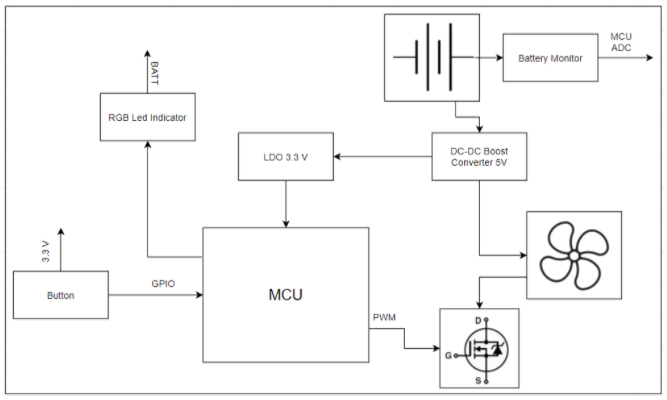
This block diagram presents the most critical components and the interconnections necessary to perform these functions.
Microcontroller (MCU)
A microcontroller is used to provide the fan's pulse width modulation, the battery voltage sensing, and the drive for an RGB LED. My goal was to use a very low cost ARM Cortex M0 or M0+ microcontroller, hopefully with support for the MBED platform which would allow code to be written in just an hour or so. A more complex microcontroller is not needed as there are very few functions for it to perform, an ARM Cortex M0 is still going to be complete overkill but they are very cheap.
The microcontroller chosen was the NXP LPC812M101JDH16J. It is an inexpensive 16 pin microcontroller available in a 16TSSOP package. This is one of the cheapest microcontrollers available on the market, despite offering relatively high performance for the price range. Microcontrollers without USB licensing/support are incredibly cheap! This package was chosen as it allows enough space for the PCB layout design to position routing traces underneath it.
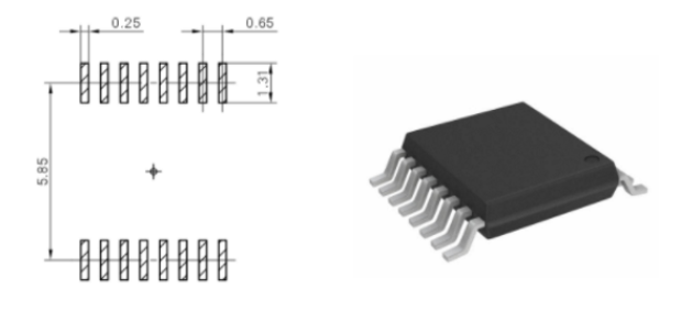
https://www.digikey.com/product-detail/en/nxp-usa-inc/LPC812M101JDH16J/568-13781-2-ND/4843237
Although there are other smaller packages available for this microcontroller and other low cost options, like the QFN 5 mm x 5 mm, such packages would utilize most of the space under the device with the exposed ground pad. This would leave no possibility of routing traces underneath the MCU on the top layer, making routing more of a challenge.
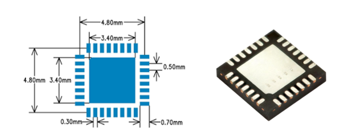
https://www.digikey.com/product-detail/en/nxp-usa-inc/LPC845M301JHI33Y/568-14091-1-ND/9449756
Fan Control
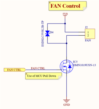
The fan needs to be controlled using a PWM signal generated by the microcontroller. However, the fan cannot be directly controlled by the MCU because the microcontroller's output pins cannot deliver the current required to flow through the fan. Therefore, an additional MOSFET is needed that is capable of driving the fan. Initially, I was looking at using a MOSFET driver IC to correctly open and close the MOSFET using the PWM signal, to reduce the RDS(on) of the FET, however I realised that with just a 5v supply there wouldn’t be a lot of difference between a gate driver controlled FET and microcontroller IO driven FET - the PWM speed would not be high enough to put much strain on the microcontroller’s IO current source/sink capabilities.
For the MOSFET, I decided to use the Diodes Incorporated DMN1019USN-13 logic level MOSFET. This transistor's source-drain resistance when a 3.3 V voltage is applied to the gate is around 10 milliohm, which is low enough to make me happy. As a result, there will only be a minimal voltage drop across the device, and the MOSFET will not heat up significantly considering the relatively tiny load of the fan. The maximum drain-source voltage is 12 V, which is sufficient for this device as the fan driving voltage is 5 V, and the drain-source current capability when 3.3 V is applied to the gate is around 8.5 A.
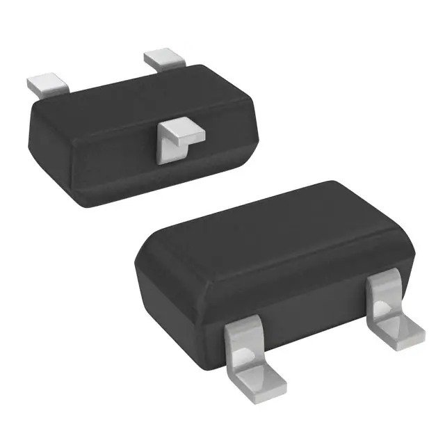
RGB LED
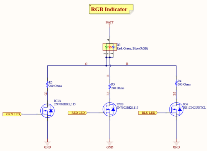
For the battery indication, a small RGB LED was chosen. The RGB LED can display the three colors required to indicate the different battery charge levels with the displayed color controlled by the MCU. The CL-505S-X-SD-T RGB LED from Citizen was chosen. The LED is available as a 4 pin SMD 0404 package. The typical forward voltage drop is 1.85 V for the red color, 2.7 V for the green color, and 2.75 V for the blue color. The maximum current is 30 mA for the red color and 20 mA for both green and blue colors. The current limiting resistors required by the LEDs will be chosen according to its specification. I could have chosen to use an addressable RGB LED here, however for the small number of units I will build the additional programming time wasn’t worth the tradeoff for a more compact board with fewer components.
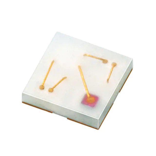
https://www.digikey.com/product-detail/en/citizen/CL-505S-X-SD-T/1642-1510-1-ND/6005950
User Input
A small tactile button was chosen for the ON/OFF and fan speed mode control selection, so the user can operate the device without difficulty. The switch needed to be small, but not too small that it was difficult to interface with mechanically. It needed to be easily accessible and simple to press. The enclosure will integrate a button that will press on the button, so having the button sitting higher off the board than other components is advantageous. For this purpose, small membrane buttons are not very suitable. I chose to use the KMR741NG ULC LFS component supplied by C & K.
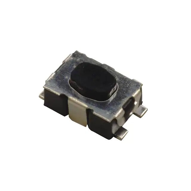
https://www.digikey.com/product-detail/en/c-k/KMR741NG-ULC-LFS/CKN10688CT-ND/6035360
Power Supply
All these devices require a power source, and appropriate voltage regulators must be chosen for this purpose. Using just one voltage regulator was not a practical solution because the fan requires a 5 V supply, and the MCU requires a 3.3 V supply requiring two separate regulators. With the voltage range of the single cell lithium polymer battery, it’s easier and more effective to step-up the voltage from the battery using a boost converter to supply 5V and then step it down utilizing a low-dropout (LDO) regulator to supply the MCU.
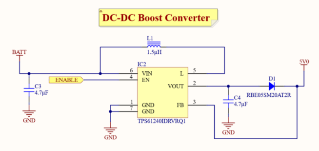
For generating the 5 V supply, I wanted a very high-efficiency DC-DC boost converter. High efficiency is required because the most significant current drawn from the battery will be by the fan, and the size of the selected small battery means that it does not have much in the way of capacity to spare on an inefficient regulator. With the serious size constraints imposed by the board area, I chose to use the Texas Instruments TPS61240IDRVRQ1 as it has high efficiency, around 93 % at the required output current for this application, is intended for battery-powered applications, and can output currents well in excess of my requirements. Its fixed 5 V output and small 6-WSON package dimensions (2 mm x 2 mm) made this converter a very suitable choice for this project. When considering a highly compact regulator, it’s amazing how much extra space the two resistors for a feedback voltage can take up when using an adjustable regulator vs a fixed output voltage regulator.
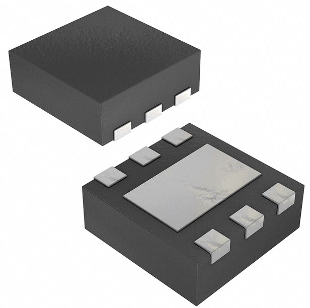
https://www.digikey.com/product-detail/en/texas-instruments/TPS61240IDRVRQ1/296-28184-1-ND/2522312
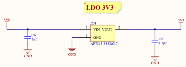
For the 3.3 V supply, an LDO regulator was chosen even though the component's efficiency is significantly lower. The LDO has a lower component count (no inductors required), and it is only needed to supply the microcontroller, which will spend most of its time in a sleep state and consuming only negligible current. I’m using the Diodes Incorporated AP7313-33SRG-7 which has a stable output voltage of 3.3 V. The LDO was chosen for its low price, small SC-59 package footprint, and fixed output voltage. Once again, it’s not worth wasting board space on feedback resistors for an adjustable regulator.
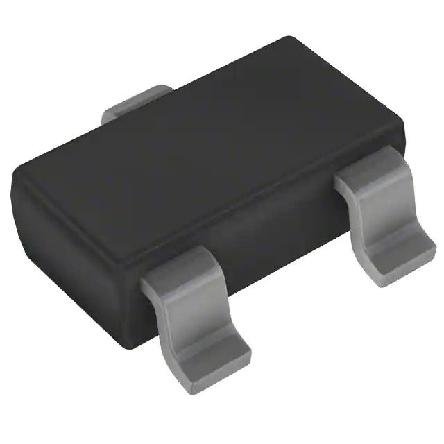
Schematic Design
Power Supply
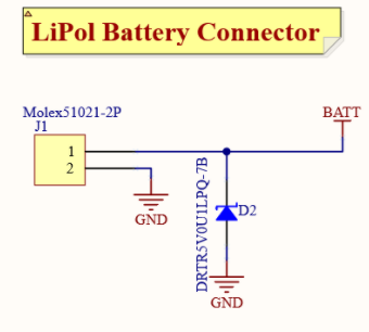
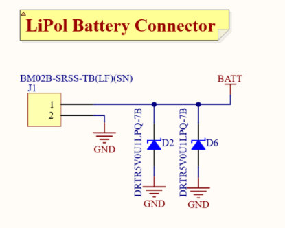
A small 0402 SMD package TVS diode, the DRTR5V0U1LPQ-7B available from Diodes Incorporated, was added to protect the circuits from ESD damage caused by human contact with the device or any voltage transients. As this device is being worn, and touched regularly as a new battery is installed a small amount of ESD protection is highly desirable.
The input and output capacitors were chosen using the datasheet recommendations, simple X5R type ceramic capacitors with a 4.7 uF capacitance value were used. No high capacitance value bulk capacitors are required because there are no components within the device that could suddenly increase current. Also, the only voltage drop sensitive device is the MCU, which is supplied from another voltage source, namely the LDO. An SMD 0806 packaged inductor with a small footprint, the 1.5 uH Murata Electronics LQH2MCN1R5M52L, was chosen because it perfectly suits our application and does not take up a lot of space. Also, a Schottky diode RBE05SM20AT2R was selected for the output overvoltage protection.
The LDO schematic design was very simple. It only required two capacitors, 1 uF at the input and 4.7 uF at the output, using components with a 0402 SMD footprint.
Battery Monitoring
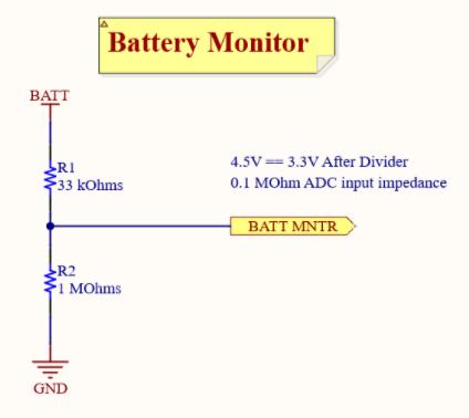
For the battery charge monitoring, I chose to use a simple voltage divider to the microcontroller ADC pin. While a battery fuel gage IC could provide a more precise measurement of battery state we have batteries that are easily user changeable, and are not charging the batteries in circuit. We also do not need a high precision of battery percentage, just a basic indication of charge compiled with a hard cutoff voltage. While the ADC pin can read the battery voltage, it cannot be directly connected because the maximum battery voltage of up to 4.2 V would damage the MCU input, hence why the divider is required. The chosen resistor values were 33 kiloohm and 1 megaohm. These values, combined with the microcontroller's ADC pin input resistance of 0.1 megaohm, provide 3.3 V to the ADC input when the actual voltage is 4.5 V. This means we can get the maximum range from the microcontroller's ADC input for all possible battery voltages without the possibility of damaging the MCU.
Fan Control
For the fan control, a simple low side MOSFET switch was chosen to control the fan speed using the MCU's PWM signal. For the fan connections, plain 1.25 mm diameter test points were used to which the fan wires can be directly soldered to. They are simple, compact, do not add any cost to the BOM, and are an excellent solution for making permanent connections. A bidirectional 5V clamping voltage TVS diode, the Micro COmmercial Co ESDSLC5V0L2B-TP, was chosen for protection. The purpose of this diode is to protect the transistor or DC-DC converter from any back EMF generated by the fan motor when current switching. An internal MCU pull-down resistor is used for both Bill Of Materials (BOM) optimisation and space-saving considerations on the pin controlling the gate.
LED Indicator
Initially, my idea was to drive the RGB LED battery charge indicator using the microcontroller's GPIO pins as current sinks. However, it was determined that the current which the microcontroller's pins can sink would generate an insufficient amount of light to be bright enough to be seen outdoors on a sunny day. Consequently, three small N-Channel MOSFETs were added to drive the RGB LED with the appropriate current limiting resistors. To save space, A twin N-ch MOSFET array (Nexperia 2N7002BKS,115) was used along with an single N-ch MOSFET (Rohm Semiconductor RE1C002UNTCL) in a small SC-89 package.
Power Control
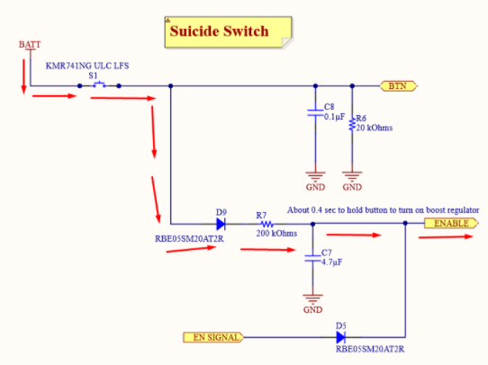
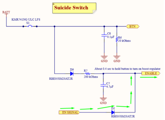
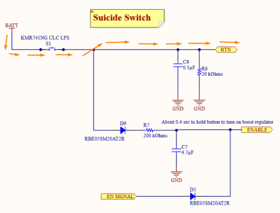
As mentioned in the introduction, I decided to use a "Suicide Switch” circuit technique to provide a way to have a single user button for power/input and also provide a way to use a hard shut off of the circuit. This circuit's purpose is to control the voltage regulator’s enable pin and also provide an input signal to MCU's GPIO pin to change the fan speed mode once the device is powered up.
If the device was OFF, it is necessary to hold down the button for at least 0.4 sec due to the RC time constant of the circuit that turns ON the boost converter and the other IC's in the device, as shown below.
When the MCU is switched ON, the circuit will hold the DC-DC converter's ENABLE pin high until the user turns OFF the device, as shown below.
When both the voltage regulator and the MCU are turned ON, the user can control the fan speed modes by sending a signal to MCU's GPIO pin (labeled BTN), as shown below.
Microcontroller
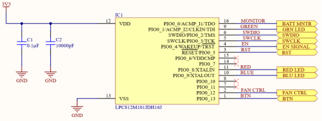
The LCP812 microcontrollers are nice and simple to use, with an internal oscillator that is more than precise enough for our application, there is very little supporting circuitry required. The supporting circuitry for this application only requires decoupling capacitors for the MCU supply. The pins' allocation was determined by iterating through different connections during the PCB layout to find the most convenient placement and optimal routing possible. The final MCU schematic is as shown below.
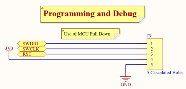
It was decided to use castellated holes at the end of the PCB for connecting the MCU programming pins. This will allow programming the microcontroller in production as well as debugging in development without taking up much valuable board space. A set of spring pin probes can be used with a jig to make contact with the programming header.
PCB Design
I really enjoy trying to cram as many components into small boards like this. It’s always a pleasure to see the jigsaw puzzle of components and tracks come together. There are a total of 33 components that all need to be placed on the top side of the PCB.
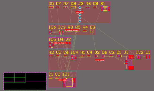
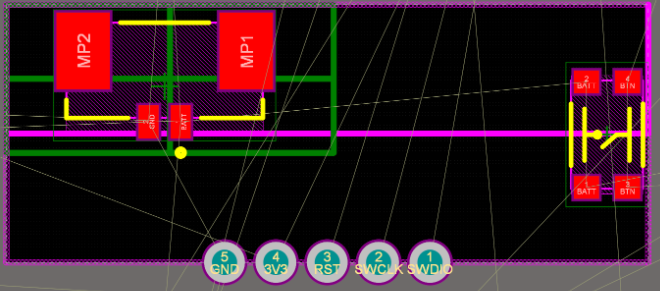
The component placement process begins with positioning the parts that had to be strictly placed in an exact location, which are the battery connector, the castellated holes for microcontroller programming, and the button. Strictly speaking, the castellated holes can move along the edge of the board as necessary but they do need to be on the edge.
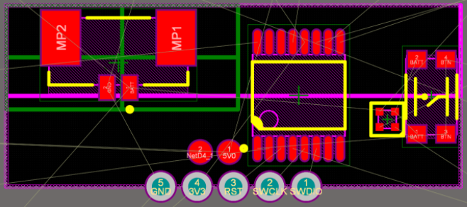
The larger components such as the MCU, the fan connection points, the voltage regulators, and the RGB LED are then placed, as shown below. Roughing in the position of critical components can make figuring out the locations of the less critical components a lot easier.
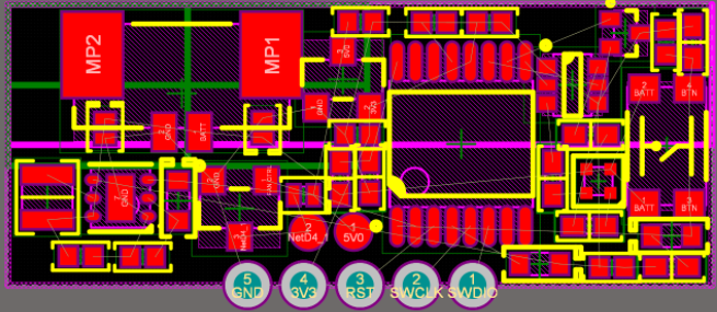
I started the design using reasonably wide 0.3 mm traces for signals and 0.5 mm traces for power and ground. These are much wider than the vast majority of board fabricators can handle, but I like to start with what I consider an ideal track width, then if there are any points with insufficient space for these traces, I can make them thinner. The same approach was taken for the vias; as you can see below, there are few wider vias in the final design.
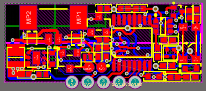
You may have noticed that there is an added additional TVS diode in this layout. During the layout process, it was easier to route two separate paths from the battery positive connection. One path to the voltage regulator and another path to the battery sensing circuit and RGB LED diode. A TVS diode is most effectively able to mitigate an ESD event if it is in series with the track that the ESD event has occurred on. By having a route away from the battery terminal that was not protected by a series diode directly, we could still damage sensitive circuitry on that path.
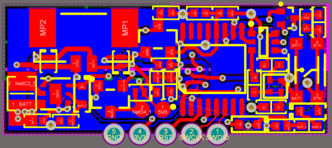
After the component placement and routing is completed, the ground layer on the bottom side of the PCB can be poured. It's important to have a fully routed board using traces, including the ground nets. If you simply fill the ground net with a polygon and hope for the best with regards to the return path, you are likely to end up with a terrible ground path.
Here you can see the component density on the PCB in the 3D view.
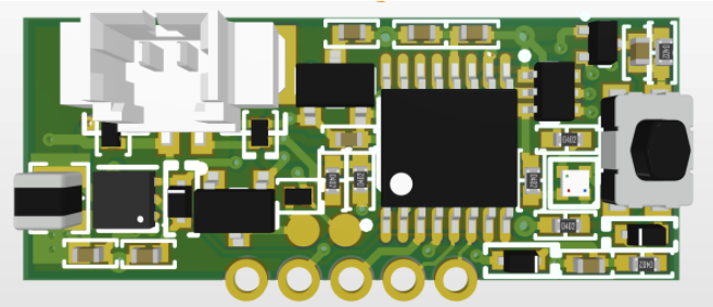
All the desired components were able to be placed without needing to remove any optional functionality to make room for routing. All the design objectives for this smart fan control board were able to be achieved.
Conclusion
This small project shows that even devices with the simplest of functions can have a complex design. The board's limited size and the specified battery connector placement necessitated the need to choose components wisely. Many microcontrollers, regulators, MOSFETs, and diodes can perform the required functions, however as the PCB area was very limited, the selected component package types were critical.
Another consideration was minimizing the component count during the schematic design. This minimization was critical because of the PCB space restrictions. Making use of array packages and making smart choices about components that will be easy to prototype with yet not take up a lot of space can make the difference between a compact board that is easy to route, and a lot of space wasted with inefficient component selection.
Implementing dense component placement requires you to think several steps ahead to correctly place components. If just one part does not fit, or it is impossible to route tracks to it, you may need to redo the entire component placement.
It is crucial when designing the layout to route every trace manually and then check that all the pads can be connected. Starting out using wide traces to see if the PCB can be correctly routed. If a trace does not fit, you can often just make it thinner, reducing it to 0.2 mm or 0.25 mm from 0.3 mm as necessary.
Would you like to find out more about how Altium Designer® can help you with your next PCB design? Talk to an expert at Altium.