Serial Communications Protocols Part 5 - SPI

In this next article in our series that is looking at different types of Serial Communication Protocols, we will be looking at the popular SPI protocol. This is one of many popular protocols in common usage that we will be looking at. We will provide a useful summary of each type’s advantages and disadvantages at the end of this series.
SPI stands for Serial Peripheral Interface. It is a serial communication bus commonly used for short-distance communications between microcontrollers and small peripherals, such as RF modules, shift registers, external flash ICs, and various sensors and SD cards. It is synchronous, which means it has a separate clock line.
The SPI protocol was developed by Motorola, although it is used in a considerable number of different ICs, modules, and devices produced by other manufacturers.
The SPI protocol allows full-duplex communications, which means that devices connected to the bus can simultaneously send and receive data.
The SPI communication protocol consists of four lines in addition to the ground, these are:
- SCLK - Serial clock (Output from master)
- MOSI - Master Out Slave In (Data output from master)
- MISO - Master In Slave Out (Data output from slave)
- SS or CS - Slave select or Chip select (often an active-low signal, output by the master)
The SPI pins can be labeled with various names depending on who the datasheet is from, so it is essential to carefully read the datasheet before starting your design.
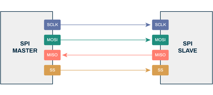
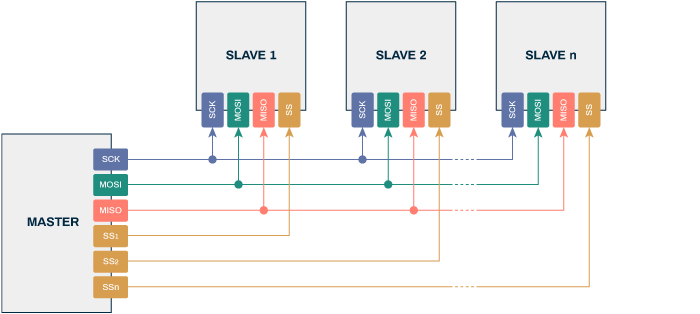
The SPI architecture typically consists of one master device and multiple slave devices that the master communicates with, which means that one set of data lines can be connected to multiple slave devices. However, the slave selection is quite different from I2C. The number of slave devices that can be used in an SPI communication network is limited by the number SS (Slave Select) or CS (Chip Select) pins you have available.
Some of the typical applications where the SPI protocol is used include:
- Temperature and Pressure sensors
- ADC, DAC, Audio codecs, Digital Potentiometers
- Touchscreens, video game controllers
- Camera lens controls
- External Flash and EEPROM ICs
- RTC (Real-Time Clocks)
- LCD
- MMC or SD cards
We will begin by looking at the communications between a master and a slave. The bus master device should configure the SPI communication clock settings to use a frequency supported by the slave device (typically up to a few MHz).
The master then selects which slave it wants to communicate with by pulling the appropriate slave select pin low, which causes that slave to start to listen. The other slaves that have their select pin pulled high will ignore the commands.
The communication principle is that the master device sends data to the listening slave device through the MOSI line. The slave can read this data while simultaneously returning data to the master device through the MISO line, where the master can read it. This is how the full-duplex data transmission occurs.
Usually, this communication involves the use of 8-bit size registers, with the first bit being the MSB (Most Significant Bit). Both master and slave shift one bit forward through the register and outputs the last bit on the clock edge.
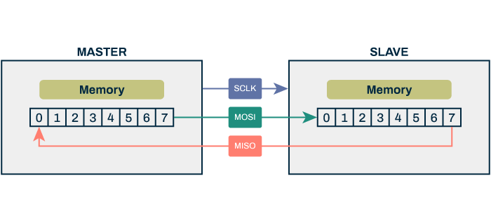
When the transmission is complete, the master device deselects the slave by pulling the corresponding slave select pin high.
Although SPI data transmissions often comprise 8-bit messaging, other word sizes, such as 16-bit, are also in common use for applications such as touchscreen controllers of audio codecs.
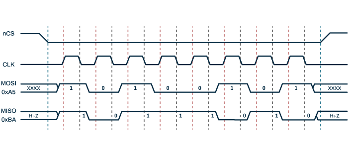
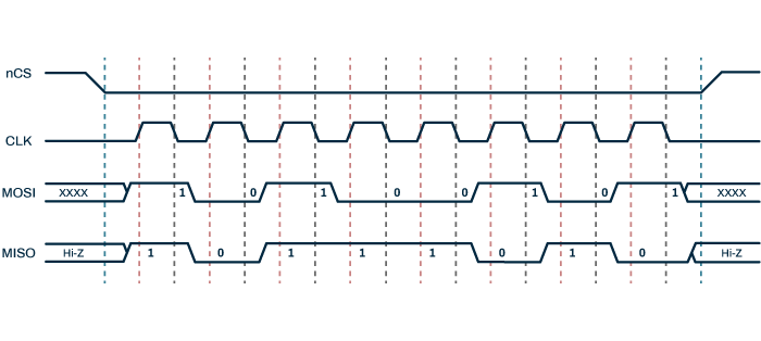
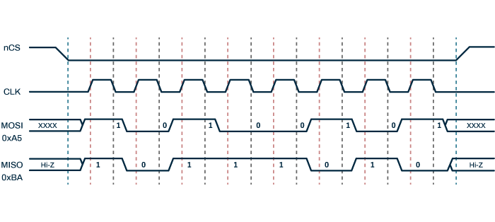
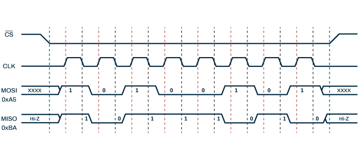
During the data transmissions that use mechanisms other than the clock speed, alternate settings such as clock polarity (which logic level represents the idle state) and phase (on which clock edge, rising or falling, the data line is sampled) can be used.
There are four different SPI modes:
| SPI Mode | CPOL | CPHA | Clock Polarity (in idle state) | Clock Phase |
|---|---|---|---|---|
| 0 | 0 | 0 | Logic Low | Data sampled on rising edge, output on falling edge |
| 1 | 0 | 1 | Lowic Low | Data sampled on falling edge, and output on rising edge |
| 2 | 1 | 1 | Logic High | Data sampled on falling edge, output on rising edge |
| 3 | 1 | 0 | Logic High | Data sampled on rising edge and output on falling edge |
The diagram below shows the timing diagrams of the SPI lines in these different modes:
One of the reasons for the SPI protocol’s popularity is that the receiving hardware can be very simple. It can be implemented using a simple shift register. This is a much easier and cheaper solution than is required to implement I2C.
Because of the high SPI bus speed, the transmission distance should be kept very low (not more than a few meters). However, it is possible to increase the maximum bus length by lowering the clock speed or using a specialized SPI driver chip.
Another solution to extend range is to use data link ICs as an intermediary stage:
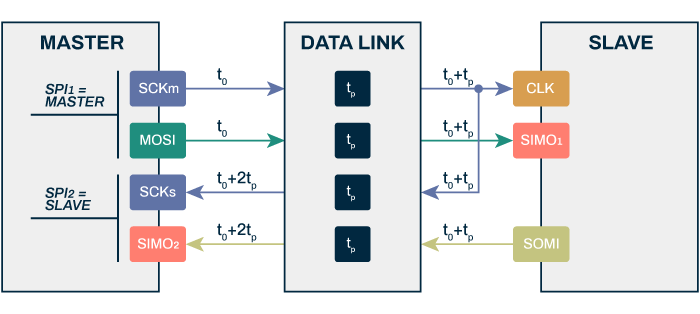
For example, you can extend the SPI communication distance by using an RS-422 data link as an intermediary stage.
Advantages of using the SPI protocol:
- Much faster than I2C
- Receiving hardware is very simple (simple shift register)
- Can support multiple slaves
Disadvantages of using the SPI protocol:
- Requires more signal lines
- Communication must be well-defined as most slave devices use their own protocols
- Master must control communications (slaves cannot talk to each other without a command from the master)
- Usually requires an individual SS or CS line for each slave device
Summary
This article has looked at some features of the popular SPI protocol and discussed some of its advantages and implementation details. In the other articles in this series, we will look at some of the alternate serial communication protocols available.
The design tools in Altium Designer® contain everything you need to keep up with new technology. Talk to us today and find out how we can enhance your next PCB Design.