Removing Noise From Analog Signals in Your PCB
On my 12th birthday, I received my very own stereo system, complete with 4 speakers, a CD changer, and a tape deck. My parents found my taste in 80s hair metal pretty annoying, but I couldn’t get over the annoying hum coming from the speakers after a CD ended.
Noise in analog systems, and analog noise in general, can present serious problems in a number of applications. Examples include systems for precise measurement, power systems, and radios. Another common example is in audio circuits, where noise can manifest itself as an annoying, audible hum. One last example is in sensors that need to gather DC or AC signals, as noise from supporting electronics can make these readings less accurate. The right design choices in these systems can prevent noise from degrading signal quality and ensure your design can withstand external noise sources.
Sources and Types of Analog Noise
Analog systems have to deal with a range of analog noise sources, some of which are unavoidable at the component level and board level. Let's look at inherent noise sources first that affect components at any signal level.
White Noise
White noise is uniformly distributed throughout the frequency domain, i.e., this noise has a flat spectrum. The best way to remove white noise from an analog signal is with bandwidth reduction. This is equivalent to reducing the measurement time for a signal and gathering more measurements, followed by averaging results. In terms of analog signals sent to an amplifier circuit, you should opt for a lower bandwidth amplifier. You can reduce the RMS noise fluctuations due to white noise by a factor N if you reduce the bandwidth of the amplifier by a factor N-squared.
Pink Noise
Pink noise, also called 1/f noise or flicker noise, has a frequency dependence that is inversely proportional to frequency. Pink noise dominates at low frequencies, but it eventually falls off to the point where white noise is the dominant noise source. Eliminating pink noise is challenging to implement at the PCB level. This may require external equipment, depending on your board’s application and the signals involved.
One common approach is chopping, which can be implemented at the IC level. In this technique, the reference signal is modulated at a higher frequency and amplified with a summing amplifier. The higher frequency components are removed with a filter, leaving behind a low frequency or DC component with higher SNR. Implementing this purely on a PCB may require the use of a frequency synthesis technique (e.g., with a phase-locked loop).
Johnson Noise
Johnson noise is better known as thermal noise, which is the random excitation of electron motion that is a function of temperature. In electronics, the DC resistance of an element increases the RMS voltage of the noise signal as Johnson noise generates a current. This type of noise is unavoidable and the only way to truly eliminate it is to run the circuit at zero temperature. This is one reason why ultra-sensitive CCD cameras for precision optical measurements are run with active cooling measures.
All of these inherent noise sources combine in components to determine a noise figure on the inputs and outputs. You can then determine the noise floor in an interconnect, below which any signal will be "lost in the noise". The noise floor can be defined in terms of the minimum equivalent input noise from all noise sources (M), the component or circuit bandwidth (B), and the component's noise figure (N):

The noise floor is like a minimum noise goal you should try to hit in your design, and it can be informative for determining how much noise reduction is required for proper device operation.
How to Reduce Noise in Analog Signals
Something to consider in answering this question is to understand how noise originated in the circuit in the first place. As was shown above, some noise sources are inherent to your components and can't be reduced at the PCB level. However, there are ways you can reduce noise at the system level, or prevent noise from being induced at the board level.
In Circuit Design
Compared to digital circuits, analog circuits are quite sensitive to noise. In addition, noise on an analog signal can be read out during sampling with an ADC, which will create an inaccurate signal reading. Analog circuit design is all about building your signal chain to ensure your low noise is carried between components. Here are some high-level guidelines to help you get started:
- Compare noise specs for your components: Make sure to dig into your component data sheets and select components that have low noise figures.
- Use filter circuits: Don't be afraid to apply filtering to reduce noise outside your desired bandwidth. This is a standard technique to limit noise outside the relevant signal bandwidth and may require a very high order filter to restrict the bandwidth to within ~10% of the desired carrier frequency.
- Pay attention to ADC sampling rates: If you're using an ADC for sampling, using a higher sampling rate followed by an anti-aliasing filter will spread noise over a broader bandwidth, which will then reduce the total noise read out by the ADC.
- Amplifier bandwidth: To reduce problems with amplifier noise, only use amplifiers that have the bandwidth you need. If you cannot reduce the bandwidth of the amplifier, you can decrease the bandwidth of an analog signal further using filtering.
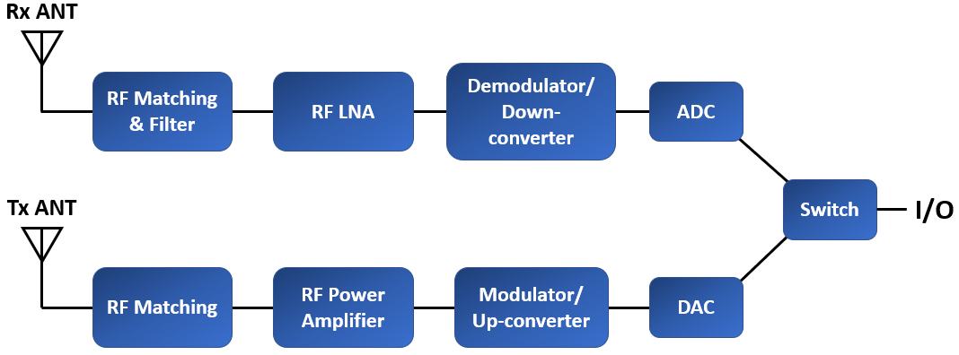
The last two points are rather important and are extensive enough that they deserve their own article. However, I've discussed some of these points on choosing the best amplifier to ensure low noise in a recent article on Octopart's blog. These points all need to be considered when creating a block diagram for an analog system. The example below shows how some of these elements are incorporated in an RF front end (RFFE) for a wireless or radar system.

In the PCB Layout
To reduce problems with EMI in an analog system and to help prevent crosstalk in an analog system, consider these guidelines for your PCB layout:
- Floorplan your board: Be sure to carefully floorplan your PCB so that your return paths for low and high frequency signals do not cross to prevent crosstalk. I've taken an approach where the signal chain flows across the board, rather than having analog sections routing back-and-forth across the board.
- Separate analog and digital sections: Keep your analog and digital sections separated and prevent return paths crossing between sections. This will help suppress noise in the digital section from being induced in the analog section as crosstalk.
- Take advantage of ground: Placing copper pour and ground planes around critical interconnects provides isolation against EMI. In addition, grounded isolation structures, such as those used at GHz frequencies, are an excellent tool for noise and EMI suppression.
- Creative routing: Coplanar waveguide routing and other unique interconnect structures provide greater isolation than RF microstrip routing. These routing styles are more common in high frequency boards, but they are useful for any critical analog interconnect.
- Shorter traces: Analog traces should be routed over shorter distances to reduce loss and ensure that the loop area associated with the return current path is as small as possible, thus minimizing parasitic inductance. This then reduces induced crosstalk strength.

Crosstalk Between Analog Signals with Different Frequencies
The first point above relates to crosstalk between analog boards operating with multiple frequencies, while the second point relates to analog boards with a digital section. Both points should be considered when designing analog boards to have low noise.
Low and High Frequency Analog Crosstalk
Many boards do not operate at a single frequency but will incorporate components operating at multiple frequencies. A perfect example is a smartphone or tablet, which will need to operate from wireless frequencies (2.4 GHz or 5 GHz for WiFi/Bluetooth) down to switching regulator frequencies (~100 kHz) and audio frequencies (up to 20 kHz). Floorplanning and isolation are important here to ensure signals do not couple to each other. Filtering is also critical here and is incorporated in many designs involving multiple analog frequencies (see the example RFFE block diagram above).
In devices with RF wireless capabilities, there is a common problem where RF signals will induce audible noise in an audio circuit through demodulation. This can be extended to any other mixed-frequency analog board that uses demodulation. In effect, the demodulation of a high frequency signal induces low frequency crosstalk in other circuits when the low frequency demodulated signal falls within the right bandwidth. Separating these components into their own sections with their own ground regions helps prevent this type of demodulating coupling.
Mixed Signal Crosstalk
It is common that a board with ubiquitous analog functionality will have some digital section. Analog and digital portions of the devices should be split into different sections above a uniform ground plane. This is a complex type of design at moderate to high frequencies (~MHz and higher) as you need to prevent return paths from crossing between sections. Placing greater distance between critical interconnects in these sections reduces the electromagnetic field strength between sections and thus crosstalk.

These aspects of noise suppression are targeted more at external EMI and other board-level noise problems, but they are vital for ensuring signal integrity in analog boards. If you have the best set of layout tools, you can implement these strategies and many more to help reduce noise in analog circuits.
Determining the best layout to ensure analog signal integrity is much easier when you have access to a great simulation and analysis package directly in your PCB design software. Altium Designer® contains the best schematic design, layout, signal analysis, and deliverable generation tools in a single interface. You can create circuits that help filter analog noise and ensure your designs are less susceptible to EMI. Once you've created your PCB layout in Altium Designer, you can quickly share your design with your team and manufacturers using the Altium 365™ platform.
Download a free trial of Altium Designer today to learn more about the signal integrity and simulation tools. You’ll have access to the industry’s best design, simulation, and verification features in a single program. Talk to an Altium expert today to learn more.
Team Up and Save
Get Special Savings When You Add a New Altium Designer Seat
