Perfect Boards Every Time (With Free Templates)
Memories Fade, but a Diamond Good Documentation is Forever
In a previous article, we took a look at how to create perfect templates for your schematics. In particular, how to craft the title block and how to style the components.
My obsession with creating pretty circuits often reaches an unhealthy degree. I often find myself going home at 9 pm having overworked myself because I obsessed over the formatting of my schematics for five hours, clocking out of the office with bags under my eyes bigger than the full moon above my head.
Creating clear, concise and readable schematics is imperative if you want the circuits you are working on to be useful long after everyone has forgotten how they work. Readable schematics are also necessary for efficient collaboration. None of Altium Concord Pro®’s wonderful features can save you from a poorly drawn circuit.
Production drawings, however, are another matter entirely.
While trained design engineers usually read schematics, your production drawings could potentially be read by technicians and workers with minimal training.
Introduced a few years ago, Draftsman®, embedded within Altium Designer®, has radically changed my workflow for the better.
Before the arrival of Draftsman, it was often necessary to include a hand-drawn template with your PCB design, as well as embed all drill tables, notes, and documentation on separate layers.
The resulting documents were hard to print, impractical to open as they still required Gerber viewers, and cumbersome to edit.
The worst part of life before Draftsman? Any time somebody required some kind of documentation, the PCB engineer had to create it from scratch, manually cross-check it against the PCB, print it to a PDF file and annotate it with external software.
It was all a bit like trying to hammer nails with a shovel.
Dreadful documentation, no more!
Your Draftsman documents should be clear and standardised. Here's how you can achieve it.
Draw me Like One of Your French Boards, Jack
So, what kind of documents should you create with Draftsman? For starters, let's take a look at what we can draw with it.
Here are the objects currently supported by Draftsman:
- Graphical objects
- Sub of Second
- Another Sub
- Line
- Rectangle
- Circle
- Arc (by centre or 3-point)
- Region
- Text
- Graphic
- Views
- Board Assembly view
- Board Fabrication View
- Board Section View
- Board Detail View
- Component View
- Drill Drawing View
- Board Isometric View
- Board Region View
- Board Realistic View
- Tables
- Generic table
- Drill Table
- Transmission Line Table
- Bill of Materials
- Layer Stack Legend
- Dimension
- Linear
- Radia
- Diametral
- Angular
- Ordinate
- Scale
- Annotations:
- Callout
- Surface Finish
- Datum Feature
- Feature Control Frame
- Center Mark
- Note
As you can see, Draftsman has bountiful features to document any kind of PCB project. Most of them are divided among manufacturing outputs of the bare PCB boards, assembly outputs, generic annotations, tables and graphical objects.
Over the years, I have found the best approach to PCB documentation is to have three different documents. The first two are mandatory, but the last one optional:
- PCB_Fabrication
- PCB_Assembly
- PCB_Mechanical
Mechanical documentation is often a necessity if you have to interface with mechanical engineers. You can detail the size and position of holes, how much the board is allowed to flex under stress, and the dimensional tolerances of bulky components such as power inductors or electrolytic capacitors.
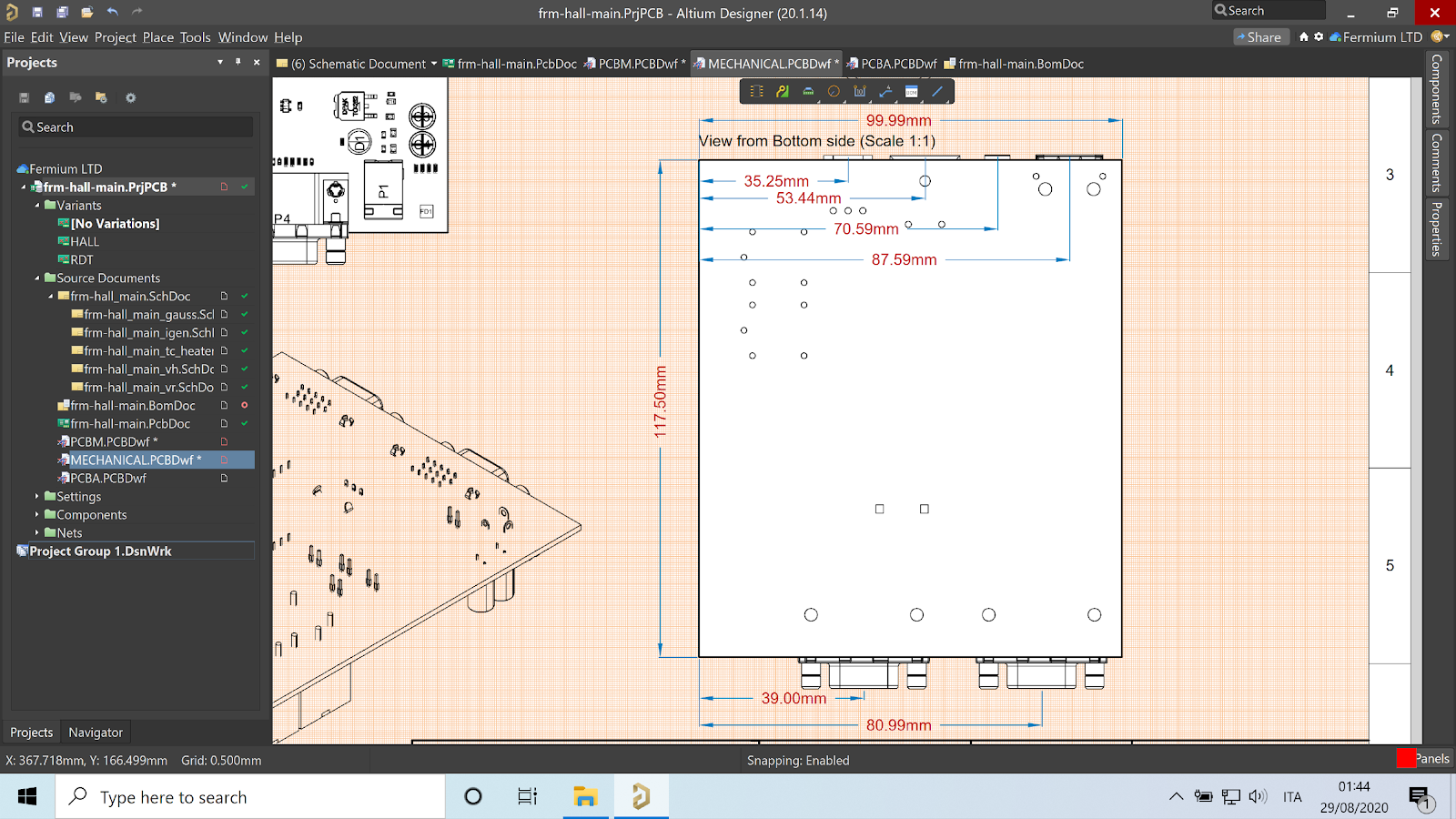
The MCAD Collaboration features of Concord Pro hosted on Altium 365™ can, however, considerably reduce the need for electronic engineers to draw mechanical documentation.
Manufacturing Drawings
A Truth Table Without Boolean Algebra
Suppose you are starting out in electronics or you are dealing with designs that are relatively simple to manufacture. In that case, you probably don't need much more than the Gerbers and a BOM to get your board manufactured correctly.
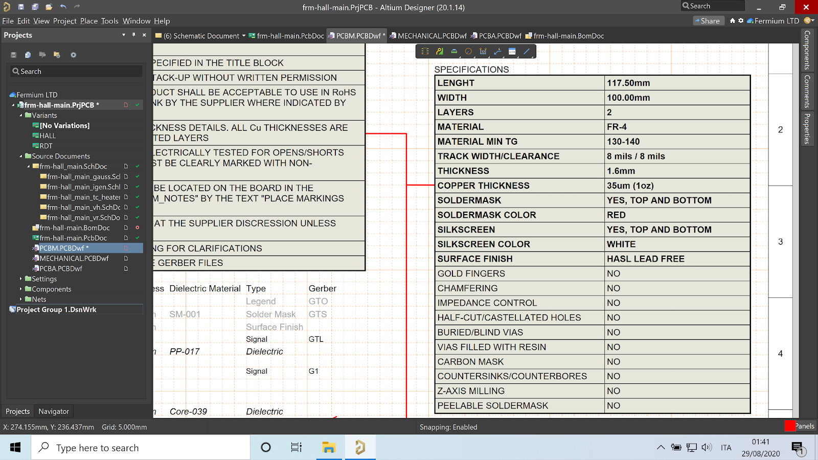
By default, most low volume manufacturers will offer you a standard process with 8 mils resolution, 8 mils spacing, 0.3mm holes, a standard 1.6mm board thickness with 32 micrometres copper, a TG (Glass Transition Temperature) of between 130 and 140 degrees Celsius, green solder-mask with white silkscreen, and a HASL (Hot Air Solder Levelling) finish.
These specifications are, however, not a one-size-fits-all solution, and in many cases, your needs might exceed them. Consider the following:
- Industrial boards often require PCBs with a high glass transition temperature to avoid excessive flexing over the temperature range.
- High-density designs require dimensional accuracy above what the standard production lines offer, as well as features such as blind vias.
- Thick copper (above 32 micrometres) might be required for high current designs.
- Controlled impedance may be required for high-speed designs.
- High-reliability boards often imply the need for a high-quality substrate from brands like Rogers, Omega, or 3M.
- You might want to specify the copper plating thickness inside your vias to reduce their parasitic resistance.
- You have particular mechanical requirements such as Z-axis milling, countersunk or counterbore holes.
- You want additional options such as edge plating, press-fit holes, via-in-pad, castellated holes, or carbon Mask.
With every project, I include a handy table in my Draftsman PCB manufacturing documents. My EMS cross-checks it, and more than once, they found mistakes in my ordering process. Just last month, I forgot to specify my boards were to be finished with HASL lead-free instead of HASL with leaded solder.
If my EMS hadn't caught the mistake by checking my Draftsman document, I would have probably ended up with a non-RoHS-compliant product, and my customer would have rejected the batch, leading to considerable losses.
Not Everything that Shines is Copper
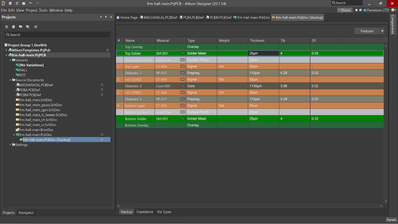
High-speed and high-current designs require particular care in the choice of layer stack. Two of the most common beginner mistakes in high-speed designs is not updating the layer stack inside of Altium correctly and manufacturing the PCB with a different layer stack than designed. In my case, here's the layer stack for the "I'm too broke to pay for high-reliability boards" offer from my favourite EMS house:

And here it is, inserted into Altium Designer's Layer Stack Manager, under the PCB Editor.
And finally, In our Draftsman drawing:
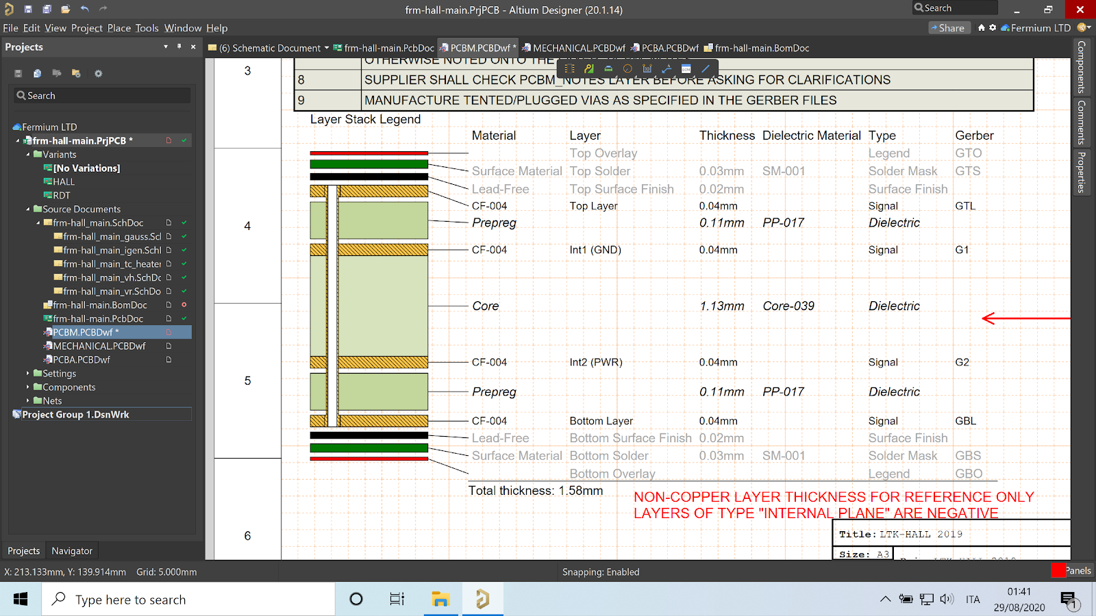
The stack in the Draftsman document is synced automatically from your PCB project, enabling your EMS house to catch any mistake for you.
One Set of Instructions Speaks Louder than a Thousand Words
Over the years, I have tweaked and refined a consistent set of manufacturing instructions. Money is always tight, and so most of my electronics are manufactured in Shenzhen. There is a common set of issues you are likely to encounter when working with Asian manufacturers. This generally stems from a difference in cultural business practices, expectations and language barriers.
One of the most common problems is conflicting specifications between different documents, such as Gerbers, emails and other types of documentation. In this case, it’s fundamental to have a single source of truth.
The following guidelines, added to the manufacturing specifications, have helped me avoid countless issues over the years:
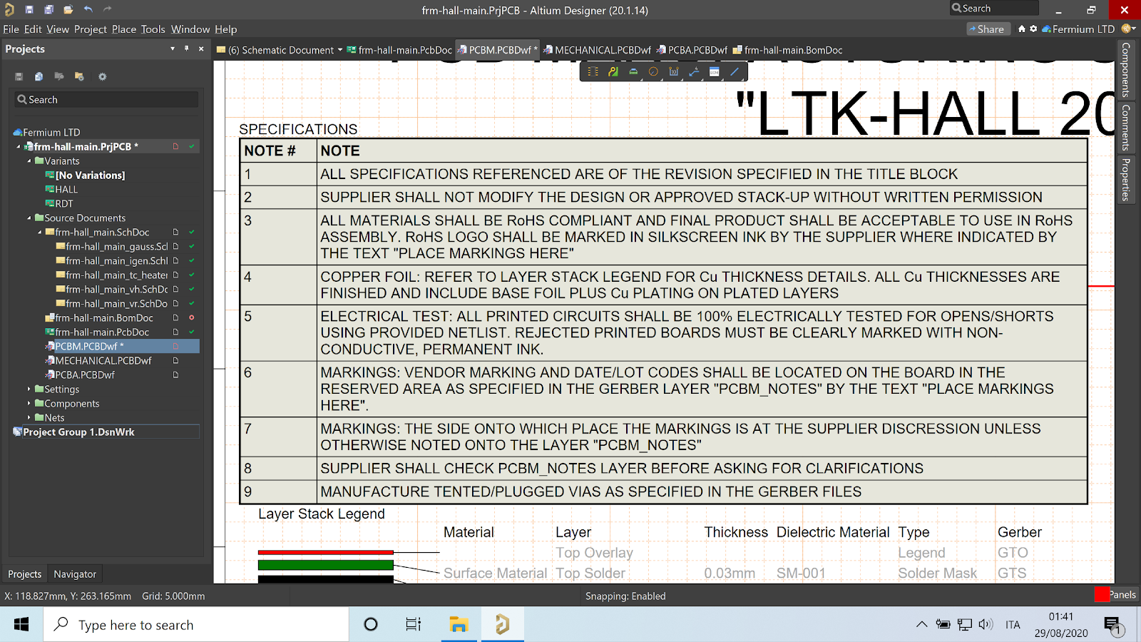
- “All specifications referenced are of the revision specified in the title block.”
- “Supplier shall not modify the design or approved stack-up without written permission.”
- Some manufacturers will do what’s cheaper and assume that’s what you want, but cheaper is rarely better. A change in specifications can alter your product performance and reliability.
- “All materials shall be RoHS compliant, and the final product shall be acceptable to use in RoHS assembly.”
- Your EMS will be responsible for sourcing most of the components as well as manufacturing and assembling the PCB. As such, they are in a prime position to be sure the product is RoHS compliant.
- “Copper foil: refer to layer stack legend for Cu thickness details. All Cu thicknesses are finished and include base foil plus Cu plating on plated layers.”
- The importance of a single source of truth is a recurring theme in this article. The copper thickness indicated in the layer stack can conflict with what has been selected during the order procedure. The layer stack should be assumed to be an accurate answer.
- “Electrical test: all printed circuits shall be 100% electrically tested for opens/shorts using the provided net-list. Rejected printed boards must be clearly marked with non-conductive, permanent ink.”
- To no-one’s surprise, the red “rejected” stickers used by some manufacturers can detach or disappear mysteriously, mostly as the holiday’s approach.
- “Markings: vendor marking and date/lot codes shall be located on the board in the reserved area as specified in the Gerber layer ‘pcbm_notes’ by the text’ place markings here’.”
- “Markings: the side onto which place the markings is at the supplier’s discretion unless otherwise noted onto the layer ‘pcbm_notes’.”
- “Supplier shall check pcbm_notes layer before asking for clarifications.”
- I always add my notes on three separate layers: one for PCB manufacturing, one for PCB assembly, and one for my personal notes. With this simple note, I save approximately two emails on every order. With different time zones, two emails often mean getting the PCB two days later than usual.
- “Manufacture tented/plugged vias as specified in the Gerber file.”
- Most manufacturers will do this already, but it’s never a bad idea to be overly specific.
I always place these notes on the first page of the manufacturing documentation:
Assembly Drawings
Using Draftsman for bare-board manufacturing is good, and all, but assembly drawings are where the software truly shines.
Altium Designer's users have created numerous scripts over the years to automate some of the most tedious tasks, but none of them comes close to matching Draftsman features and ease of use.
Similar to the manufacturing drawings, I like to provide a clear set of instructions on the first page:
- "All specifications referenced are of the latest revision unless otherwise noted."
- "Supplier shall not modify the design without written permission."
- "Refer to Excel BOM for up-to-date component information."
- "The BOM in this document is purely an AID to assembly operations and may not have the most up-to-date data or all approved component alternative."
Gosh, Harry, What's the Anode?
I have a challenge for you. Pick a board you designed, preferably one that has already been approved for production. Open both the assembly drawing and the Gerbers using your favourite Gerber viewer.
Now, tell me the orientation of all diodes.
Not so easy, right? In some cases the orientation is clear, but in many, you'll almost have to guess.
Virtually all large companies in the electronic sector have some sort of internal guidelines documenting how diodes should be represented. Smaller businesses and freelancers, however, often leave it to custom and chance.
I have had to solve this issue for multi-billion-dollar companies.
Here is my take on it.
Draftsman can mark pin one with a dot in the assembly drawings, like in the following image:
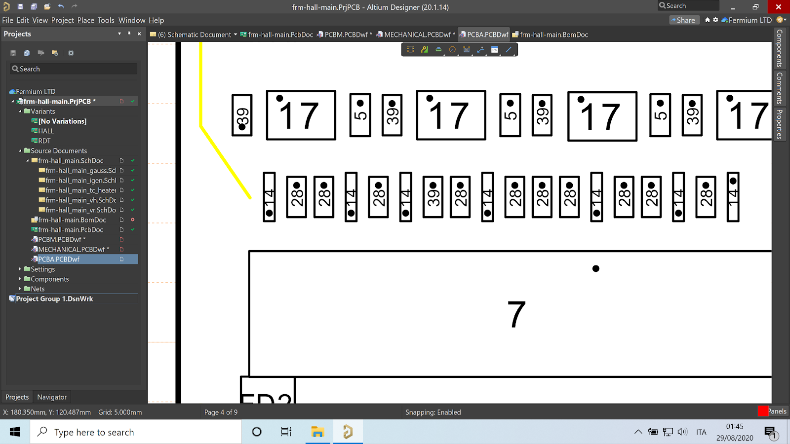
Intuitively, the dot should go where the "pointy end" (cathode) of the diode is. I have asked multiple colleagues about this, as well as friends who have no knowledge in electronics, and almost everyone gave the same answer: dot equals pointy end.
IPC-7351B, the main standard that deals with SMD footprints, seems to agree with this conclusion.
Engineers who mainly draw schematics have a different perspective on the issue. It is common to feel that pin one should be on the anode and pin two the cathode to mimic the current flow when the diode is forward-biased.
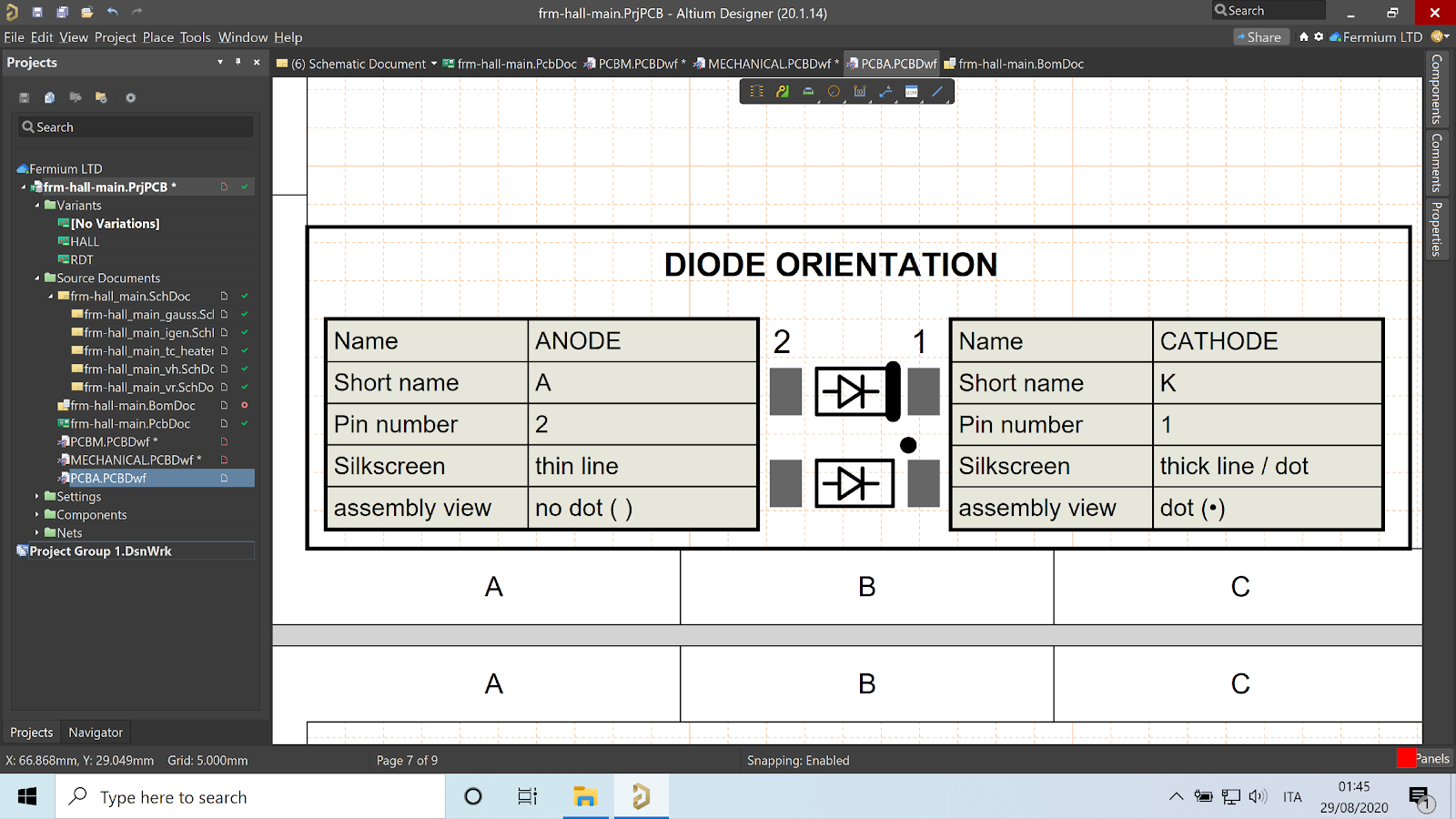
For the drawings to display correctly in Draftsman, the cathode must be pin 1 in the footprint. Having mismatched schematic and footprint pinouts is sure to be a source of trouble, so it follows that the schematic should have pin 1 on the cathode as well.
Additionally, it is usually necessary to have an indication of the diode's orientation on the silkscreen layer. Even if it's too small to manufacture, your EMS house will be able to read it when they view the Gerbers and zoom-in.
In my case, I mostly draw my footprints similar to the way Mark Harris does for his wonderful Celestial Library, with a diode symbol underneath the component body and an outline with a thicker line on the cathode side.
I have found this approach works wonders on boards of all shapes and sizes, although you might want to drop the outline for high-density designs and smaller case sizes.
Mark does, however, draw his diodes with pin 1 on the Anode. His approach makes the schematics more intuitive at the expense of the manufacturing documents.
To be absolutely sure there is no confusion, the diode orientation should always be noted in the assembly drawings where it can be easily cross-referenced.
Losing Lawsuits is for Losers
Under most NDA agreements, the only documents considered confidential are those explicitly marked as such. Don't be the fool whose lawsuit for breach of contract gets dismissed before it even begins!
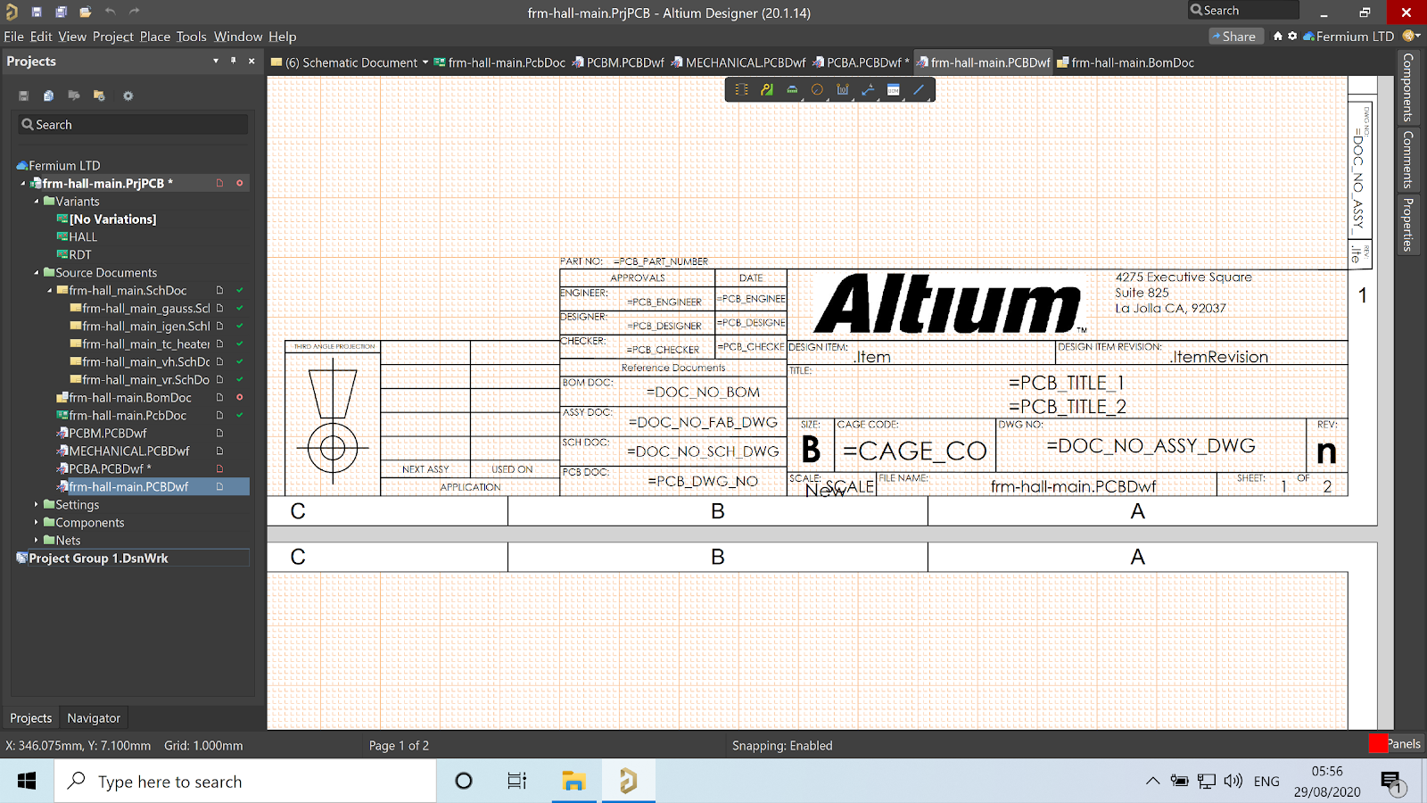
It is a good idea to include "confidential" in a professional-looking title block:
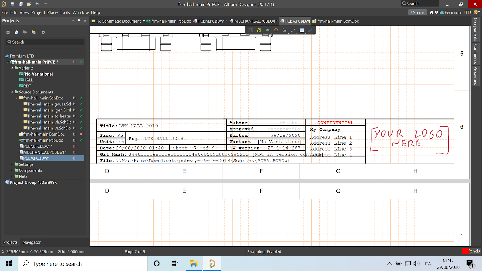
Altium Designer offers you standard ANSI and ISO templates, but those have been created with mechanical drawings in mind. Many of the notes and fields do not reflect the needs of the electronic industry; for example, "Deburr and break all sharp edges" doesn't make much sense for us!

If you use Concord Pro on Altium 365 you will also have access to more PCB-centric templates by default.
Huaqiangbei Won't do it for Me
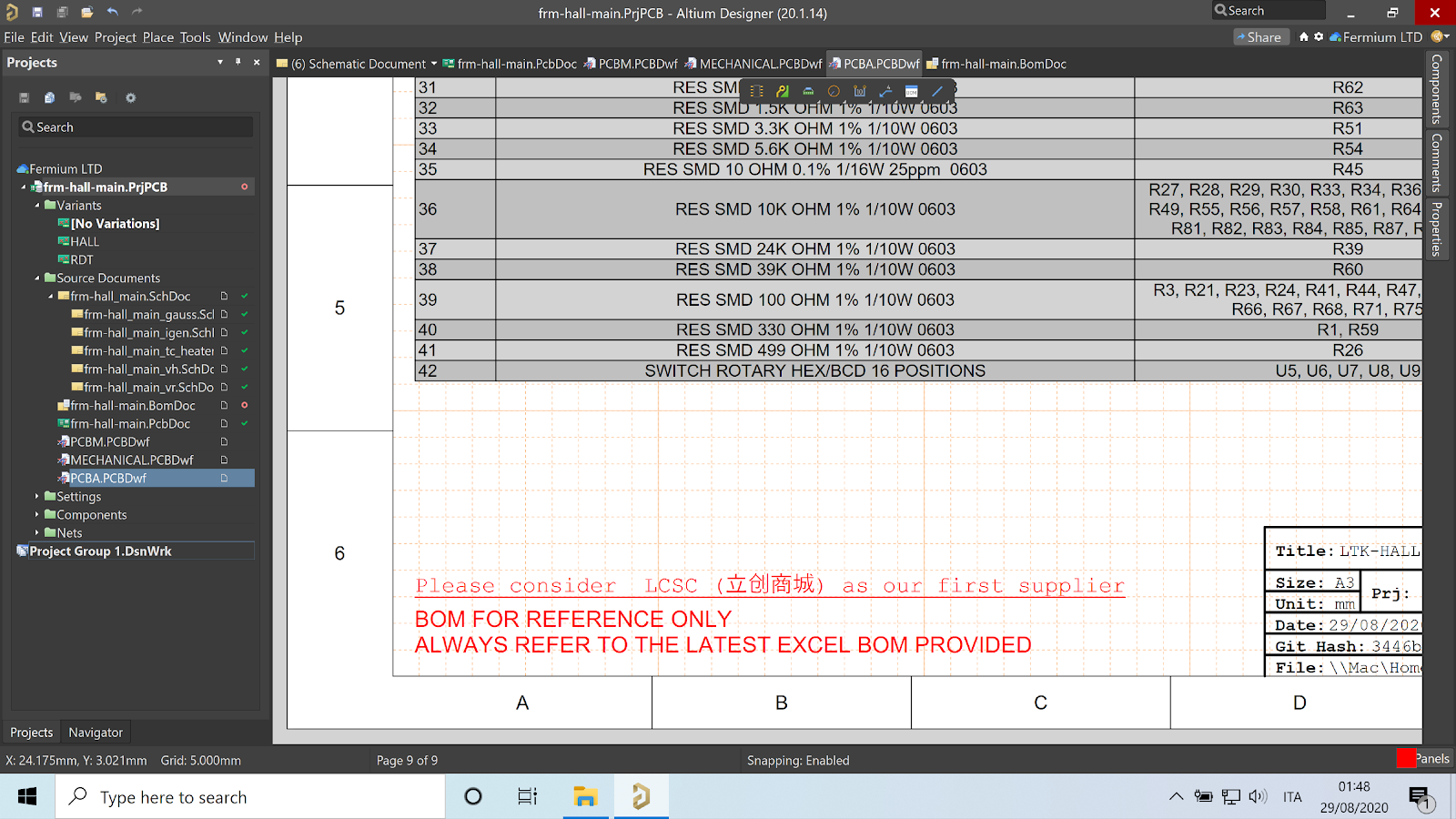
Your assembly documentation is also the perfect place to include instructions for purchasing. In my case, I want my Shenzhen suppliers to buy my components from LCSC first, so I always add a little note to the BOM page.
Get Your Free (Handsome) Draftsman Templates
I have created five A3 templates for you:
- A generic sheet template, containing only a title block
- An assembly sheet template that includes the diode orientation diagram
- A PCB manufacturing document template
- A PCB assembly document template
- A PCB mechanical document template
You can download them on the Github repository AltiumTemplates.
Please note they don't include a revision field as I use Git hashes instead.
Sharing Templates With Your Organization
No matter how good your template is, it will be of little use if your company is not consistent in its adoption.
Using Concord Pro on Altium 365, you can share your Draftsman Templates and manage their revisions.
Using the managed template feature, it's incredibly easy. Altium Concord Pro comes with a series of industry-standard ANSI and ISO templates. Still, you can add your own by dragging and dropping from Windows Explorer or creating a new item (right-click, new item) and then uploading the template (right-click, upload).
Just remember to save your Draftsman document as a sheet template or document template, not as a standard draftsman document.
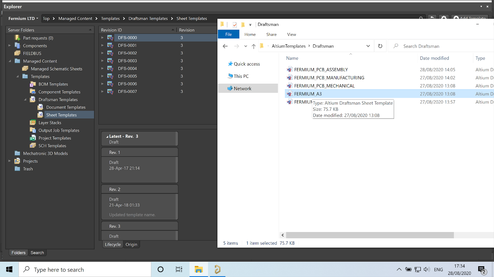
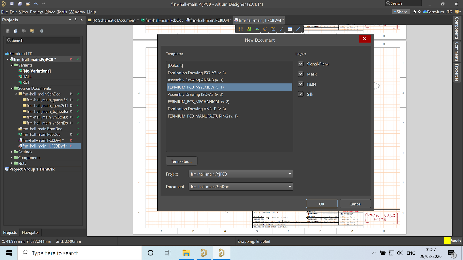
Once you have done so, your Draftsman Templates will be available Organization-wide when creating a new document.
Further Reads
Altium's documentation has a wonderful introductory tutorial to the IPC standard, something that normally you'd have to pay big bucks to get access to, masqueraded as a Draftsman tutorial. You can find it here.
Mark Harris has written an article about dimensioning draftsman documents, as well as one about project templates you might want to take a look at.
You should also check out the official Draftsman documentation and the extended Draftsman managed template documentation.
Conclusions
Ironing shirts can be boring and tedious until you get a proper high-pressure steam generator.
A bit like that, Draftsman takes all the repetitive, eye-drying tasks of PCB manufacturing documentation out of the equation, leaving you with only the fun bits. Printing them and sniffing the sweet smell of inkjet in the morning, that's what keeps me going.
Concord Pro on Altium 365 allows you to manage and share Draftsman Templates with your whole organisation, making sure all engineers are on the same page - pun intended. Improvements in the documentation can be easily applied to all managed projects, ensuring you build upon your experience over the years.
Would you like to find out more about how Altium can help you with your next PCB design? Talk to an expert at Altium.
