Optical Interconnects in PCB Design: Progress in 2020 and Beyond

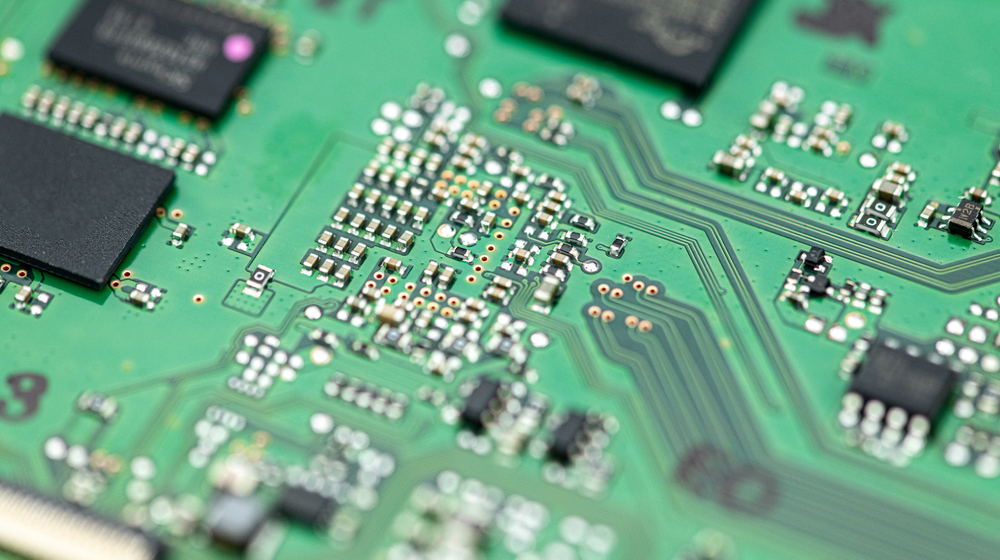
Imagine shrinking all the equipment shown in the above image down to a single chiplet. Getting a set of networking equipment shrunk down to that size is a bit extreme, but new technologies are continuing to push electronics in that direction. The modern world is continuing the trend of greater data creation, transfer, storage, manipulation, and consumption that began when PCs first hit the market. Many enabling technologies have driven this trend and one prominent technology is optical communications.
Sure, we’re talking about fiber optics, but we’re also referring to integration of optical interconnects onto integrated circuits and, eventually, PCBs. Chip-to-chip optical interconnects have been around for decades, but today’s technology is bringing silicon photonic integrated circuits (PIC) closer to being commercialized than ever before. With this being the case, what is happening on the PCB?
Today, the landscape for photonics and optical interconnects is creeping ever closer to the PCB-level, and it pays for board designers to know how to accommodate these advanced technologies. Today, optical interconnects are being constructed from COTS components, but tomorrow, it’s possible these interconnects are printed directly on a PCB substrate.
Challenges in Optical Interconnects for PCBs
Optical interconnects are simply the optical analogue of an electrical interconnect; they provide routing for signals on or between PICs. Everything that is deployed commercially in the field is all-electrical; the optical portion of an interconnect ends at the fiber transceiver input on the PCB. Going partially or fully optical simultaneously solves many signal integrity problems and enables higher (bandwidth) data rates. Optical interconnects and photonics are also enabling advanced applications, some of which have been demonstrated quite recently. Some examples include:
- Quantum computing: Silicon photonics provides an alternative to superconductors for use in quantum computing, and it may be the key to easing cryogenic requirements. The use of photonics in developing new quantum computing architectures was recently demonstrated and reported in IEEE Spectrum.
- Artificial intelligence: This is one contemporary application where high compute power is required in parallel. Optical interconnects and ICs enable higher data transfer between different components and systems in a data center.
- 5G and future telecom networks: Optical interconnects and photonic components reduce the number of required electronic components in edge servers and base stations by providing a direct interface with fiber backhauls.
- Lower-power computing in the data center: Everything that happens today in data centers requires high compute power. Photonic systems are one option for providing higher data transfer and processing rates without increasing power.
PICs are making an appearance in all of these applications, but there is a common set of challenges to overcome before optical interconnects can appear directly on PCBs:
- Material platform: Some scalable material platform is needed to fabricate interconnects between photonic circuits. His is still an active area of research, and it remains to be seen which optical materials can be adapted into a planar process for PCB fabrication.
- Manufacturing: In addition to the material platform, there is still the question of whether or how the PCB manufacturing process will need to change to accommodate optical interconnects.
- I/O interfaces: This is where the chip meets the board, and it’s where the fate of optical interconnects on PCB substrates will be decided.
Some candidate optical interconnect technologies from the recent past include polymers and embedded optical interconnects, where glass fibers are embedded directly in the PCB substrate. However, these do not match so well with the current best-in-class technology for optical I/O interfaces. Therefore, the future of printed or embedded optical interconnects will depend on how optical I/Os on photonic chiplets are structured.
Today’s I/Os for Optical Interconnects
Today’s I/Os for PICs and other optical components still resemble fiber transceivers, where an optical cable plugs directly into the I/O to provide an optical connection. However, early tests of these technologies show that they can provide throughput reaching into the Tbps regime with excellent signal integrity.
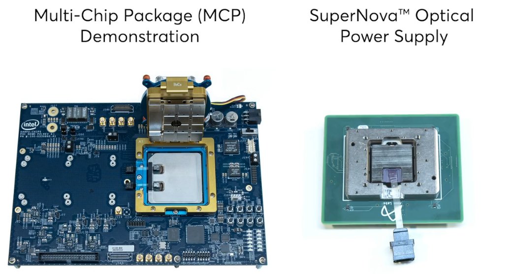
Perhaps the most advanced I/O structure and the closest to commercialization are the results from DARPA’s Photonics in the Package for Extreme Scalability (PIPES) program. Headed by researchers from Intel and Ayar Labs, optical I/Os coming directly off the semiconductor die can be used to provide connectivity between PICs without bulky transceivers on the board. The image below shows how this looks for a multichip module (left) and a driver chiplet that acts as an optical power supply.

The I/O side of ICs for optical interconnects is becoming more capable thanks to advances in silicon photonics. The present optical I/O style is rather unwieldy, and there are currently two candidates for integration into the PCB substrate:
- Polymer interconnects: If we go the route of polymers, we may find a material that can be printed in the standard process or with an additive process directly onto a PCB. All that needs to change is the interconnect style on the die to couple light into these structures.
- Embedded glass interconnects: In April 2020, embedded optical interconnects with a pin header-style I/O connection were announced by a research team at Tokai University. Their fabrication process might be useful with other I/O interfaces and terminations in future PICs.
Time will tell whether these interconnect styles or some alternative will be commercialized alongside with state-of-the-art I/Os on upcoming photonic components.
Although major progress in SerDes and other high speed electrical interfaces have repeatedly set back commercialization of photonics, newer technologies are demanding photonic components and optical interconnects, and they’ll need to be integrated at the PCB level. As these new technologies are commercialized, Altium Designer® will be there with the design tools you need to create cutting-edge circuit boards that support photonic systems.
In addition to design tools, Altium provides all its users with access to the Altium 365™ platform, making it easy to collaborate with other PCB designers throughout the project lifecycle. We have only scratched the surface of what is possible to do with Altium Designer on Altium 365. You can check the product page for a more in-depth feature description or one of the On-Demand Webinars.
