Noise Margin Analysis Part 1

In a previous article, I described the various aspects of noise margins, their sources and why it is necessary to sum up all the noise margins for every logic component utilized in a given design.
This two-part article addresses why noise margin analysis is a critical element within the design rule creation process, and how that analysis is incorporated into the final design rule set. Part 1 addresses the three elements comprising a design rule set; Vcc and ground bounce and ground and Vcc offsets. Also described is what needs to happen when current loads are so high that it’s not possible to put enough copper in the power path. Part 2 addresses ground and Vcc drops in IC package power leads; reference accuracy; signal losses in traces; thermal offsets and effects; terminator noise and power supply variance. Also included are examples of noise margin analyses.
Design Rule Set Creation
The three elements that comprise a design rule set include:
- Timing Analysis
- Power Subsystem Design
- Transmission Line Rules
Each is described below.
Timing Analysis
When a PCB is being designed, it’s important to feed the path-length delays on the routed signal traces into the timing analysis tools that are being used for the design process. Timing analysis is first done at the pre-route stage after all of the components have been placed such that they satisfy thermal requirements, manufacturability goals and the routability of the PCB itself. Since, at this stage in the process, the PCB has not yet been routed, the path lengths are estimated by calculating the Manhattan distance between the points in each net and then supplying this information to the timing analysis tool.
Note: Manhattan length is the shortest path that a wire can have when it must be connected using only segments that are confined to either the X or Y axis. Calculating this length is done by subtracting the X coordinates of the two points from each other and the Y coordinates of the two end points from each other and then summing up the two dimensions. In dense PCBs, this X-Y discipline is mandatory to fit in the most wire in each layer and to ensure that crosstalk does not occur between adjacent signal layers.
Power Subsystem Design
Design rule creation for power subsystem design has been described at length in previous articles. Here, it will be shown that the allowable ripple on the power supply voltages is often determined by how much of the noise budget can be consumed by ripple. CMOS logic outputs in particular short each data line to Vcc or Vdd when the output is a logic 1. The result is that ripple on Vcc or Vdd appears on the logic lines with little or no attenuation.
Figure 1 shows the noise sources in an ECL supercomputer design.
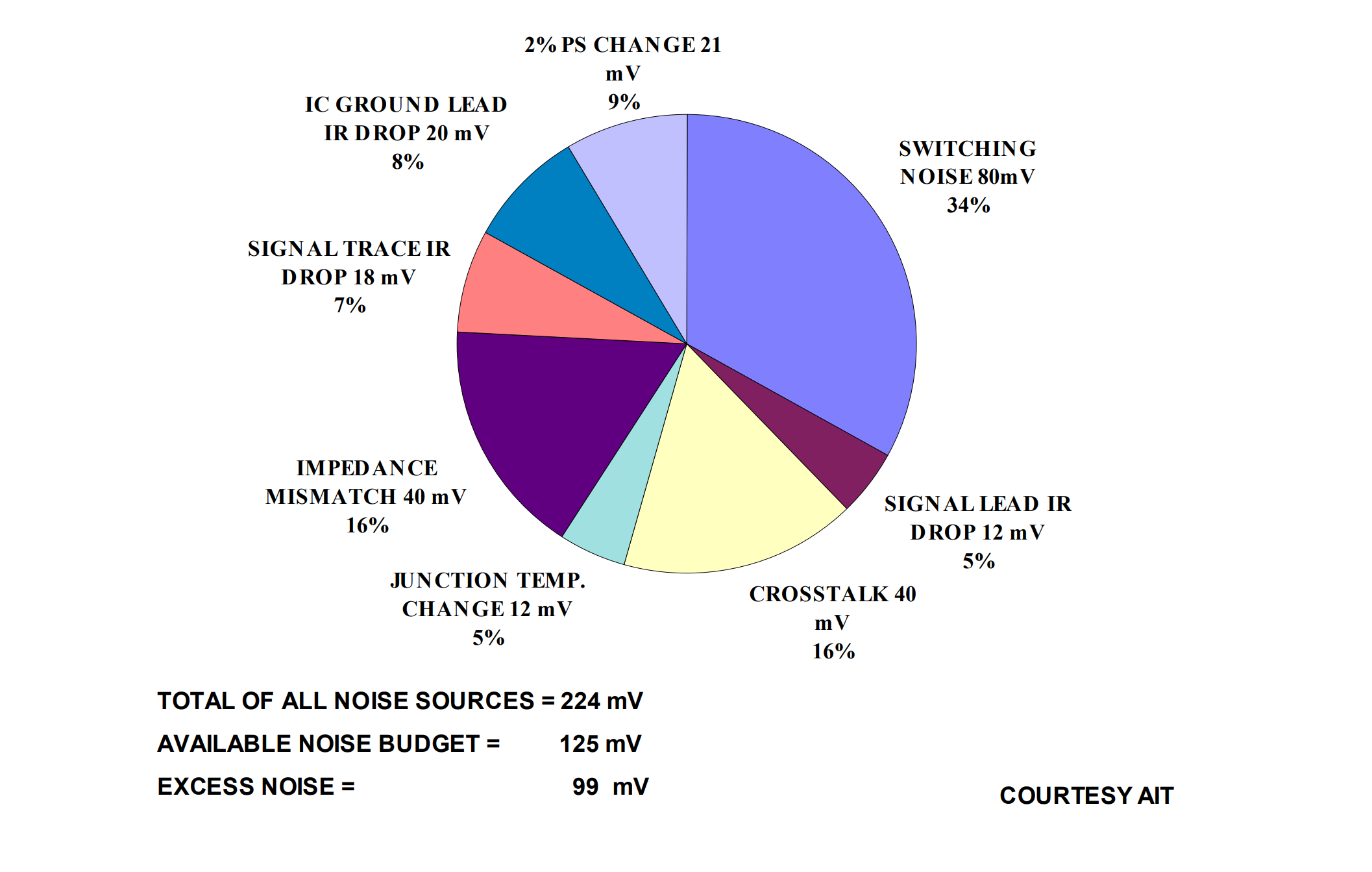
This pie chart is used as an example because ECL is the only logic family that has noise from all ten possible noise sources. Unfortunately, the analysis shown in this chart was done after the design was completed rather than before it was started. Specifically, it was done to determine why the supercomputer was unable to perform in a stable manner and was therefore deemed “flaky.”
At the bottom of the figure is the sum of all of the noise sources and the noise budget available. In this instance, the excess noise was 99 millivolts, which is too much. SSN (simultaneous switching noise) turned out to be the largest noise source. The noise was caused by ICs being packaged in a carrier or lead frame that had too much inductance in the Vcc and ground paths.
The only remedy for this problem was to redesign the system with the ICs in a package that had acceptable Vcc and ground bounce characteristics (i.e., low parasitic inductance). Unfortunately, this remedy could not be absorbed by the company and both the product and the company disappeared. If the proper noise analysis had been done prior to launching the design, the flaw would have been detected, a better IC package selected and the design stable from the onset.
The Noise Sources
Since reflections and crosstalk have been covered in-depth in previous articles, the remainder of this article will focus on the other noise sources as listed below.
Vcc and Ground Bounce
Vcc and ground bounce are the shift in the Vcc and the ground rails on the IC die as they relate to the respective levels on the PCB planes. This type of unwanted transient is most often the result of single-ended logic drivers charging and discharging transmission lines. Figure 2 illustrates the way in which Vcc and ground bounce are created.
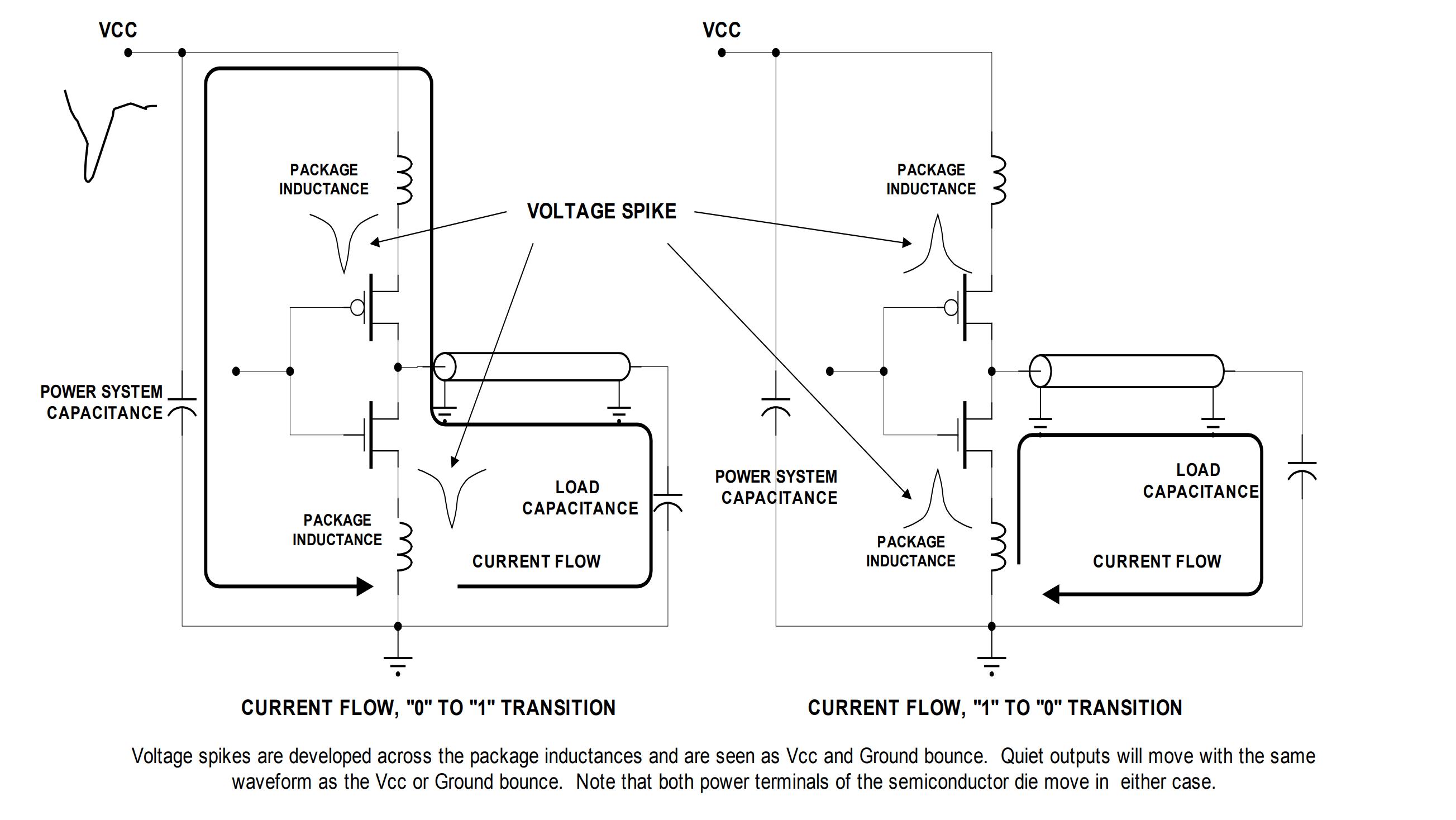
The left side of this figure shows the current path for the required current to charge up the parasitic capacitance of the transmission line along with the parasitic capacitance of the loads as the transmission line is switched from a logic 0 to a logic 1. The right side of the figure shows the current path associated with discharging parasitic capacitance as the logic line switches from a logic 1 to a logic 0. These transient currents are the primary source of the SSN. The inductance shown in the diagram includes the inductance of the vias that connect the IC power leads to the power planes.
It can be seen that the Vcc terminal of the IC die is driven negative with respect to Vcc on the PCB power plane during a logic 0 to 1 transition. All of the terminals of the IC are driven negative at the same time. This is Vcc bounce. The effect is that the voltage spike appears on all quiet inputs and outputs. If the voltage spike is large enough it can result in a logic failure. During the transition from a logic 1 to 0, the ground rail of the IC is driven positive with respect to ground on the power plane. This is ground bounce.
This spike also appears on all lines and can result in a logic failure.
Equation 1 can be used to calculate the magnitude of the voltage transient resulting from the change in logic states.

The voltage drop occurs across inductors only when the current through them is changing, or more precisely, when the EM field traveling through them is changing.
Table 1 lists the lead inductances of some typical IC packages. The reason there is a wide spread in inductance is because the leads in most packages have widely varying lengths.
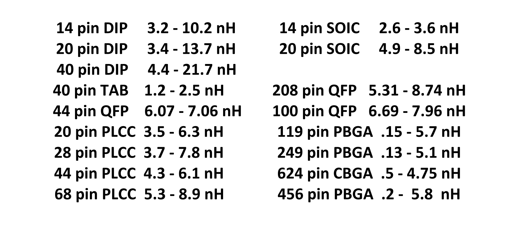
To get some sense for the magnitude of Vcc and ground bounce that can occur, a simple calculation can be performed. For example, a 20-pin DIP (dual in-line package) is used. The power pins on this package are on the corners and have an inductance of 13.7 nanoHenrys per power pin. The delta I, in this case, is when the logic state changes from 0 to 1. This is 50mA for a single output and the delta time is 2 nSEC for a 5V HCMOS component. Applying these values to equation 1 results in a voltage spike of 34 mV. When all eight bits of a bus are simultaneously switching from 0 to 1, the voltage spike is 2.74 volts. When the rise time is changed to 1 nSEC, the spike is 5.48 volts. Switching transients such as these drove the change from DIP to PLCC (plastic leaded chip carrier) packages. Component manufacturers that attempted to increase logic speeds while keeping the tried and true original packages found that their parts no longer worked. As noted above, a problem in an IC component package cannot be solved by making changes to the PCB.
The foregoing also applies to the widely-used QFP (quad flat pack) packages. While the inductances are not as high as those in DIP packages, the width of data buses is much wider than eight bits. In these instances, the failures resulting from SSN are infrequent because the worst-case spike only occurs when all of the data bits are changing simultaneously from one logic state to the other. This occurs only once in 2N times where N is the number of data bits in the bus. Before the advent of better component packaging, this was the cause of designs being labeled as “flaky.”
Ground and Vcc Offsets
Ground and Vcc or Vdd offsets are the voltage drops that occur along the path from the power supply to the using circuits as a result of current flowing in the real conductors that make up the path. These conductors include the planes of the PCB and the power connectors. To the extent that the ends of the logic paths span these conductors and their associated voltage drops, the logic levels may be shifted such that the noise margins become eroded. Figure 3 shows the measurements of these drops in a real PCB and provides some sense of the magnitude of these voltage drops.
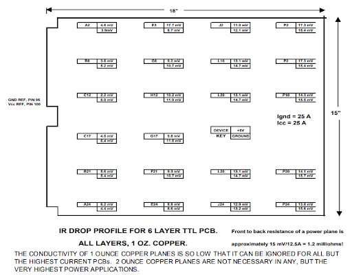
The measurements in Figure 3 were made using a millivolt meter to measure the drop in voltage from the point where the power and ground entered the PCB on the left edge to the power and ground pins of all of the ICs on the board. This current was consumed uniformly from the front of the PCB to the back. It can be seen that the total voltage drop in the Vcc plane along with the voltage rise in the ground plane was approximately 15mV. Whether or not this is a reasonable voltage drop depends on the logic family involved and its noise margins. In this instance, the component was TTL with 400 millivolts of noise margin that could tolerate 15 millivolts of offset. In cases where there is not as much tolerance for noise, (here, it is a 1.5 CMOS logic family) techniques must be employed that reduce this drop. An obvious solution is to add more metal in the form of multiple planes or create thicker planes.
There will be voltage drops in the connector pins that bring power into the PCB. It is imperative that the DC voltage drops that occur at this point be calculated before the system is designed in order to ensure that there are enough power pins.
Note: When the connector pin voltage drop calculations are executed, it is important to use the end-of-life resistance of the connector contacts. Failure to include this data can result in systems that work properly when they are new, but fail as time goes by and the connector contacts degrade.
From time to time, there is a question regarding the resistance of power planes. Specifically, the context is whether signal voltage drops will be developed through the planes between adjacent parts. Using the data within Figure 3, a simple calculation can be performed. As the evidence shows, the 25 amp current resulted in a total voltage drop from front to back of approximately 15 millivolts. Since the current was consumed uniformly front to back, the average current over the length of the PCB was 12.5 amps.
Ohm’s law states that the current in amperes is equal to the voltage in volts across a resistance divided by the resistance in ohms. Based of this, the front to back resistance of either plane in Figure 3 is 1.5 milliohms. This is a very small resistance and validates the assumptions made in transmission line modeling that plane resistance is negligible compared to the resistance of traces.
What Happens When Current Levels Are So High That It’s Not Possible to Put Enough Copper in the Power Path?
Many of today’s high-performance products use high power components such as microprocessors, DSPs, network processors and FPGAs that simultaneously require very high currents and low power supply voltages. This results in the need for low voltage drops in the power structure at the same time that the noise margins shrink. This creates the need for far more metal in the power distribution system than is practical.
There are two solutions to this problem:
- When DC offsets exceed the noise margins of the logic, differential signaling can be used. This is how the offsets between the ends of Ethernet paths are addressed.
- Reduce the magnitude of the current that flows in the power distribution system. This is accomplished as follows:
- Instead of producing the final voltage with a power supply and delivering it through the power distribution network at a very high current, an intermediate voltage such as 12, 24 or 48 volts is generated. This is delivered to the regulators on board that are next to the consumers of the power. These regulators step the voltage down to the final voltage. As a result, the current that must pass through the connectors is greatly reduced. At the same time, the final voltage is delivered through a very short path to the loads.
Next: Part 2—more sources of noise; noise margin analyses and incorporating the analyses into the design rule set.
Have more questions? Call an expert at Altium or continue reading about adopting signal integrity in your high-speed design process.