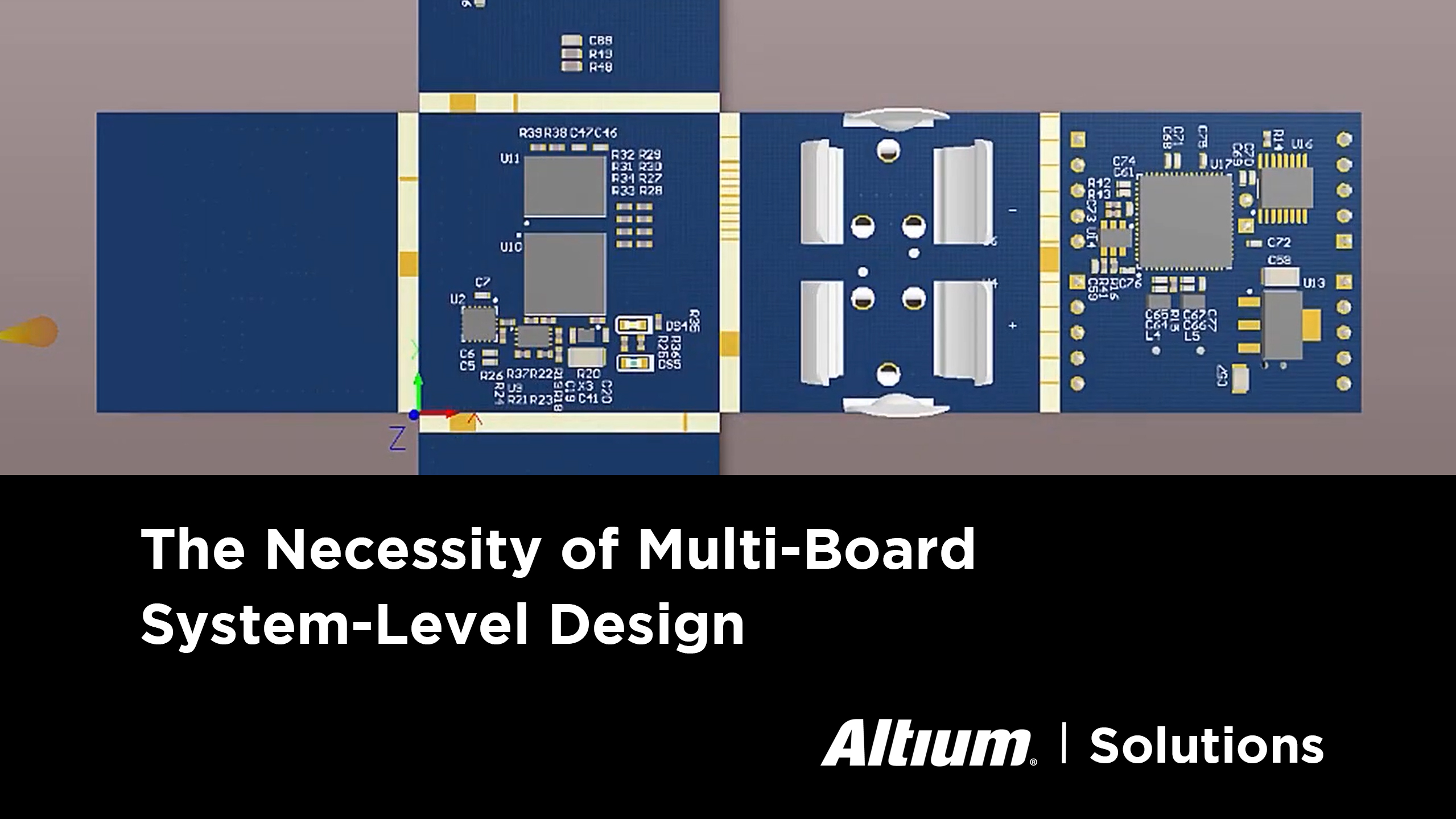
Designing PCBs for Interconnected Multi Board Systems in Altium Designer

If you open up some of your favorite electronics, you’ll find they are multi-board systems or multiple PCBs connected together with cables and ribbons. In the past, PCB design software has treated each board in the system individually without considering important circuit board design issues like power distribution and grounding, high-speed routing, mechanical assembly, and thermal demands.
Design software has caught up to the demands of professional circuit board designers, but how do you choose the PCB design package you need to create your next multi-board system? The answer lies in considering all the available functions and features in your PCB design software. When you use Altium Designer, you’ll have access to a full suite of design tools that are naturally adapted to multi-board PCB design. Your circuit board design tools will integrate with your multi-board design features in a single program.
ALTIUM DESIGNER
The most powerful, modern, and easy-to-use PCB design tool for professional use.
For years the standard system design workflow has been to develop the individual PCB design, and then physically fit its prototype build into the full system mockup. With today’s complex designs offset by demands for reduced design schedules and budgets, the old workflow has become a logjam due to the time and expense of continual prototyping. Successful system design still requires working with all the boards together in order to verify their fit and connectivity. However, the question is, how can this be accomplished in a more timely and productive fashion?
In the old days, you’d have to manually track connections between printed circuits boards in a multi-board system with MCAD tools or by hand. Now, ECAD software can link the layout and schematic for each circuit board and apply design rules to each section. With the right design software, your standard routing and rules checking tools will be spread across each PCB in a multi-board system. This is how Altium Designer makes multi-board PCB design easy and helps you build advanced electronics.
The Necessity of Multi-Board System-Level Design
Historically, PCB design has been handled on a board-by-board basis. The traditional design flow may have included a high-level multi-board design, but the actual boards were designed individually. Not only was this the standard practice, but the older design systems didn’t have the capabilities for multi-board design, to begin with. Once the PCB designs prototypes were built, then the boards would be tested for form, fit, and function with the other system boards. Corrections would then be made in the next revision of circuit board designs to get the boards to work correctly together.
This approach no longer works for the advanced technologies that are being created today. The requirement for more system level design is increasing while the need to shorten design cycles is increasing as well. To keep up with these requirements, the traditional methods of system-level PCB design need to be updated with CAD tools that can handle the complexities of multi-board system level design.

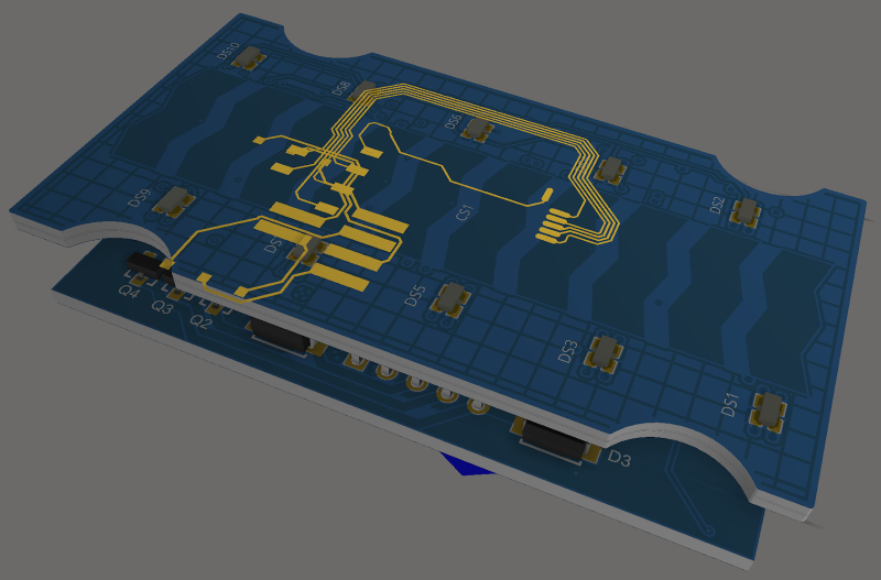
The right multi-board PCB design features help you quickly identify nets in your 3D PCB layout.
Getting Started with Multi-Board PCB Design
Multi-board PCB design follows the same process and designing a single circuit board. Components are added to schematics for each board, and the schematics are captured as an initial layout. Plane layers, vias for layer transitions, pads, and copper traces are all designed for each board in the system. The magic in multi-board PCB design comes from defining electrical connections between each board, and in designing the arrangement of the various circuit boards in 3D.
Moving Through Multi-board PCB Design with the Right Software
You’ll need the following tools for effective multi-board system-level design and PCB layout:
- Schematic editing and capture
- Hierarchical and multi-channel schematic design
- Layer stack manager for each board with via links between layers
- PCB layout and routing in 2D
- MCAD tools to define the circuit board arrangement
The multi-board PCB design process begins with schematic capture, transitions to a complete printed circuit board layout for each board, and ends with a complete documentation package that describes all aspects of your multi-board system. Along the way, your circuit board design software will need to integrate data from a number of sources, including your components, layer stack, and all other aspects of your circuit board.
Once it comes time to plan your multi-board system for production, you will need features that allow you to generate consistent documentation and assembly instructions for any manufacturer directly from your design data. Printed circuit design and manufacturing can finally be addressed in a single program when these important tasks are integrated into a single program with a consistent interface.
- Altium Designer and a team of experts are here to show you the finer points of multi-board design techniques and help you design successfully.
Learn more about multi-board design with PCB expert Ben Jordan.
- Rigid-flex boards are inherently multi-board systems, and your design software should be adaptable to working with either type of system. See how your design software can support rigid-flex and multi-board systems.
- Any multi-board manufacturer needs a complete documentation package. You shouldn’t have to use word processing software to create a bill of materials and assembly instructions. Your design software should create this documentation for you.
Learn more about the documentation your manufacturer needs for fabrication.

Once each circuit board in the system is designed and the PCB layout is created, you can arrange your boards in 3D with MCAD features.
Multi-board PCB Design Needs MCAD Integration
Any multi-board PCB design requires mechanical verification to ensure each circuit board will fit together properly. Boards that connect with pin headers or other connectors need to satisfy tight mechanical constraints in order to prevent collisions between components. The best way to do this is with MCAD features, which allow you to view each circuit board in 3D, as well as your system of boards.
Unfortunately, most low-quality printed circuit board design platforms do not include these features alongside your standard printed circuit design features. You’ll be forced to export your design to a mechanical design program, where you’ll lose the ability to co-design your printed circuit features. This is why you need to use a design application that integrates all these important features into a single application.
Why Multi-board PCB Design Needs Integrated ECAD/MCAD Design
When your ECAD features are integrated into a single platform alongside MCAD features, you won’t need to switch between programs to complete important mechanical design tasks. All your design rules will be checked and handled in 3D as you prepare your mechanical design. This lets your produce the most accurate 2D and 3D layouts in a single program and prepares them for the manufacturing process.
- When your MCAD features integrate with your important ECAD features, you’ll have a complete set of design tools for creating powerful multi-board systems. Learn More about 3D MCAD tools for multi-board PCB design.
- MCAD and ECAD tools are critical for ensuring your new design can be produced correctly and that it will fit in its enclosure. When you’re preparing assembly drawings, you can create extremely detailed drafts for each circuit board in your system with Draftsman.
Learn More about viewing your board topology with Draftsman.
- When your layout is finished and it’s time to create manufacturing drawings, you need to generate all deliverables for multi-board PCB assembly. This includes multi-board assembly drawings, bills of materials, Gerber files, and much more. Learn More about multi-board BOM generation and preparing for production.

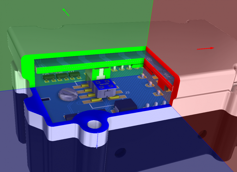
Multi-board design works best when your ECAD software contains MCAD tools. You’ll have the power to quickly cut into different board sections and verify mechanical constraints.
Multi-board PCB Design, Layout, and Manufacturing in a Single Platform
Multi-board PCB design can be a difficult task that requires the best design, simulation, verification, and documentation tools on the market. While other printed circuit board design platforms split these tools into different programs, you’ll only find all these features in one application when you use Altium Designer. This unique printed circuit board design platform offers a modern workflow that helps you complete the most advanced design tasks in a single program.
The 2D and 3D CAD tools in Altium Designer allow you to fully verify the accuracy of your system-level design and multi-board PCB design before you send your board out for production. The unified design environment gives you access to every design feature you need without switching between multiple programs. In addition, you’ll be able to generate every manufacturer deliverable you can imagine, and all within a single design platform.
Altium Designer Makes Multi-board PCB Design Easy
The multi-board PCB design functionality in Altium Designer uses a 64-bit multithreading architecture, giving Altium Designer the power to handle any challenge. While the simple, intuitive interface in the schematic editor lends itself to first-time users, it is also one of the most powerful and versatile schematic capture applications available today. It has been created to handle the most complex hierarchical and multi-channel designs. Multi-board PCB design capabilities are built into Altium Designer, and you can even import your design into popular MCAD applications for enclosure design and modeling.
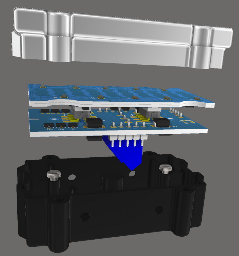
The capability to support the transition from ECAD to MCAD within Altium Designer serves as a major factor for Multi-board designs. Because MCAD systems do not consider electrical rules, the interaction between ECAD and MCAD allows the placement of densely packed components with collision checks. The Multi-board Assembly Editor also shows how the PCBs plug into one another. Altium Designer exports 3D STEP files and the correct Step enclosure data to ensure that boards do not exceed specified height profiles.
- The unified environment in Altium Designer places all of your design tools in a single program, and the underlying rules-driven design engine makes them uniquely adaptable to multi-board design. Learn more about Altium Designer’s unified design environment.
- The hierarchical, multichannel schematic editor is a natural choice for multi-board PCB design. Schematic capture is quick and easy with Altium Designer, and you won’t need a separate program for printed circuit board layout. Learn more about hierarchical, multichannel schematic design in Altium Designer.
- Multi-board system design is much easier when 3D design that unifies MCAD and ECAD capabilities are included in a single program. This allows you to verify the electrical and mechanical functionality of your embedded system simultaneously. Learn more about MCAD/ECAD integration for multi-board PCB design in Altium Designer.
With Altium Designer, the only thing you need to worry about is designing top-quality electronics. With Altium Designer’s multi-board PCB design technology, you’ll have full control over all aspects of your multi-board PCB design process, and you can verify your system-level design before you send your circuit boards out for manufacturing. It’s time to take control over your multi-board PCB design: it’s time to try Altium Designer.
Altium Designer on Altium 365 delivers an unprecedented amount of integration to the electronics industry until now relegated to the world of software development, allowing designers to work from home and reach unprecedented levels of efficiency.
We have only scratched the surface of what is possible to do with Altium Designer on Altium 365. You can check the product page for a more in-depth feature description or one of the On-Demand Webinars.
