How to Design a Boost Voltage Regulator

In this series of articles, we’re looking at the design and implementation of the main types of power regulators and converters you might use in an electronics project. I gave a graduate engineer who I mentor a series of requirements to demonstrate each of these types and have recorded the results here so you can work through the same exercises and hopefully come up with the same results.
For the next switching power supply project from my Projects Ideas for Student Engineers article, the requirements were a little bit different. This time my graduate engineer had to design a voltage regulator that could increase the voltage. For this type of task, arguably, the most popular design choice would be to use a DC-DC Boost Converter.
My requirements for this design were:
- Input Voltage 1.0 ~ 3.5 V
- Output Voltage 5.0 V
- Output Current 100 mA
You will see that DC-DC boost converters have a different topology from buck converters, and most often, they are used with battery-powered devices. Most of the time, the voltage that the battery can supply will not be sufficient to power up the majority of ICs, so a voltage boost is required.
One of the most common examples is when you need to use one or two of the very common AA, AAA size batteries cells, or maybe single-cell Lithium-ion or Lithium Polymer batteries. Typically, the ICs in your design will require a 5 V DC power supply to work correctly. A simple Zener diode nor a series or shunt linear regulator will be able to do this.
The purpose of a switching boost power supply is to be able to supply 5 V of output voltage when the device is powered by a single AA, AAA, AAAA, B, C, or D size battery or two such batteries in series. These batteries will typically supply 1.5 V each, providing 3 V when two are connected in series. Devices powered by such batteries will not use a tremendous amount of current, so having a 100 mA output current capability should be sufficient for most typical applications.
A DC-DC boost regulator IC was meticulously chosen by my graduate engineer with my supervision. The selected DC-DC boost regulator IC being the Analog Devices LTC3429.
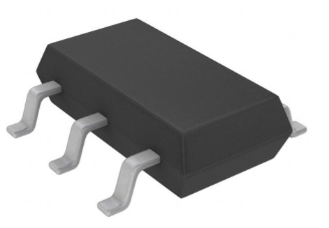
The LTC3429 component is a high efficiency 500 kHz adjustable output voltage boost converter. This converter’s stipulated operating input voltage range is from 0.5 V to 4.4 V, which ideally fits the design’s specified input voltage. This regulator’s output voltage is adjustable from 2.5 V to 4.3 V. However, the output voltage can be increased up to 5 V if an additional Schottky diode is included.
This particular boost regulator was chosen because of its high efficiency for the specified output current (Up to 96%). But the downside is that this regulator may be quite expensive, with a unit price of a few dollars when ordering small quantities. This regulator also can be obtained from Farnell, Mouser, Arrow, etc. Most of the Analog devices integrated circuit prices are high if we compare with their counterparts; however, the quality of their products is very high, which I believe makes the investment worthwhile.
Besides, you will see that this regulator comes with useful additional functions, such as:
- Low voltage start-up - this regulator can turn on with the supply voltage as low as 0.85 V. This means that if the supply battery becomes discharged to lower than 0.85 V, then there is a chance that this regulator would not start. However, our design requires a minimum input voltage of 1 V, which is more than enough.
- Soft-Start - this functionality prevents the regulator from turning on the output voltage for 2.5 ms from when the supplying power source (battery) is connected to the device. This soft-start function allows the regulators’ oscillator to stabilize at the correct frequency before it starts operating as a switching power supply.
- Anti-ringing control - this functionality prevents high-frequency ringing from occurring on the SW pin, which minimizes the EMI produced by the regulator.
- Short circuit protection - this functionality allows the circuit to be shorted out without damaging the regulator. It immediately discharges the internal capacitor in such a way that shuts down the IC, hence protecting both the regulator and the circuit.
Schematic design
You will see that the schematic design was not as challenging to design as it was for the high current DC-DC buck controller, which was capable of outputting 6 A. This design is for low current battery-powered applications, so the component selection was not as strict. You can see the circuit design recommendation from the data sheet below:
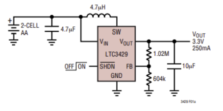
Most of the design decisions were taken straight from the schematic.
As a first step, the output voltage feedback resistors were calculated using the formula shown below, which was provided in the data sheet:

High resistor values were chosen to ensure good efficiency at light loads.
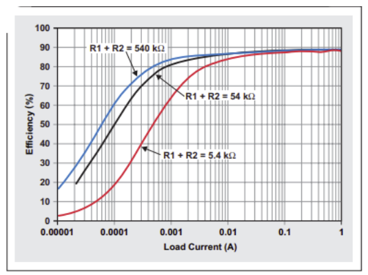
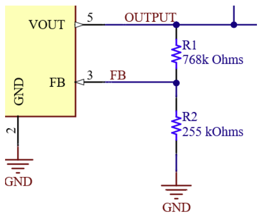
A value of 255 kΩ was chosen for R2, then the value of the R1 resistor was calculated using the formula below.

_2.png)
As this is not a standard component value, a more typical 768 kΩ value was chosen for the R1 resistor.
The variability of input and output capacitor selection is relatively high in this design. As the current of both the input and output is not high, the maximum current values for the capacitors do not matter that much.
Low ERS multilayer ceramic capacitors should be used to minimize the output ripple. Capacitors marked as type X5R or X7R are recommended. As for most applications, output capacitors with values ranging from 4.7 uF to 15 uF are sufficient. An output capacitor with a 22 uF capacitance value was chosen as it is the recommended value that provides an extremely low output voltage ripple and an improved transient response.
For the input capacitor selection, a low ESR capacitor is also required to minimize any input switching noise and reduce the peak current drawn from the battery. As the batteries are renowned for their low noise levels, a capacitor of 10 uF is sufficient for virtually any application.
Bearing in mind that the input capacitor DC voltage rating can be as low as 4 V or 6.3 V as the input voltages are relatively low. However, it is recommended to use at least double the DC voltage rating for the output capacitor. The ceramic capacitors tend to have a DC bias effect, which can significantly lower their capacitance at particular voltages.
The inductor value was taken using the following graph, which was provided in the data sheet:
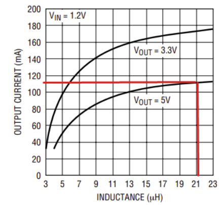
An inductor with a pretty high inductance of 22 uH was chosen because we want to maintain the regulator’s efficiency at the required output current.
The selected inductor was a TDK general-purpose inductor, the SLF7032T-220MR96-2PF component, which has the capability to handle the required output current, and their cost is low even if you buy them in small quantities.
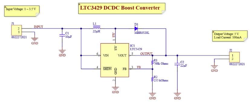
As for the Schottky diode, which is needed to generate the required 5 V output voltage, the ON Semiconductor MBR0520L component identified in the data sheet recommendations was chosen. This diode is not that expensive and can be bought for a few cents.
The inverted shutdown pin (SHDN) must be pulled up to VIN because we do not have any external controller or supervisor IC to control the regulator. We want it to be working when any power source within the acceptable input voltage range is applied.
The chosen connectors were the Wurth Electronik 0022272021. These are cheap and pretty practical as you can’t connect them the wrong way around.
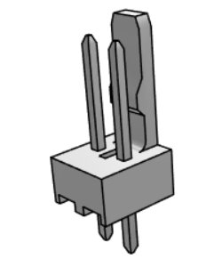
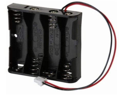
However, you can choose any connectors that you like. As part of the device’s design, you can use these battery sockets, which means your batteries are already connected in series. There are sockets available for 1, 2, 3, or 4 cells (or even more if required), and they each cost a few cents.
Below you can see the fully designed LTC3429 boost converter schematic.
PCB Design
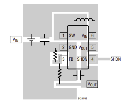
As for PCB design, the goal was to achieve the shortest possible current loops. For reference, the following design provided by the data sheet was taken:
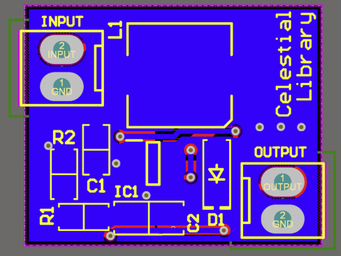
First of all, the component placement was done to ensure a compact PCB design and achieve a small board area, given that this is for a low current application.
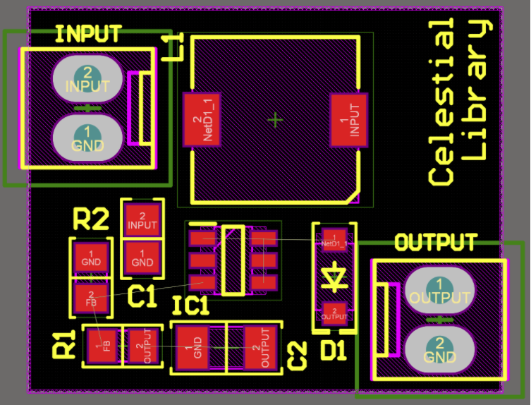
As a second step, the PCB was manually routed to carefully track the current loops. This helps you see if the design of your current loops can be improved:
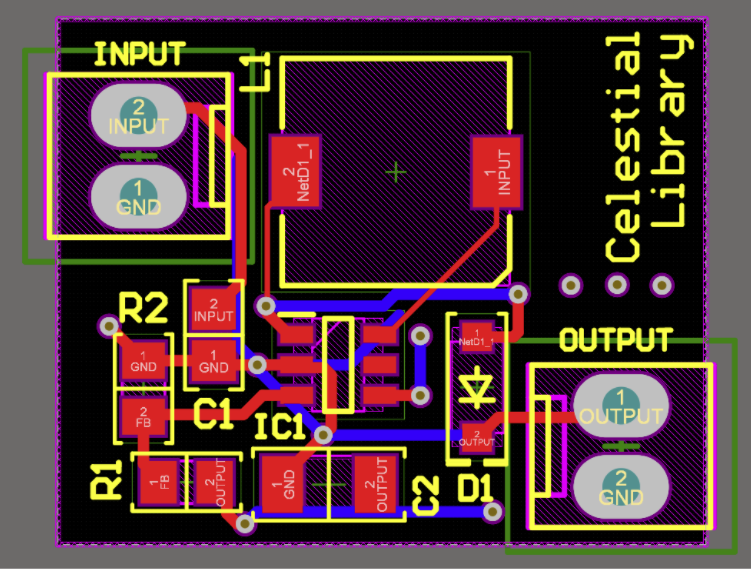
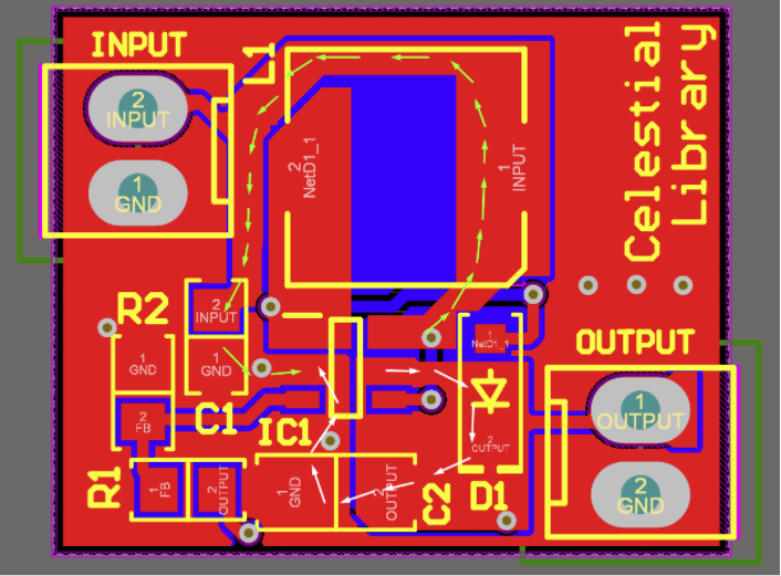
As a third step, the polygons and planes were added to the design:
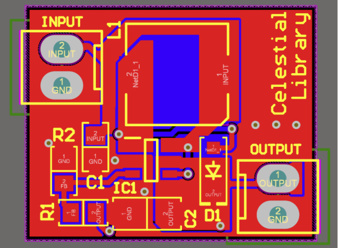
The Input and Output current loops shown on the PCB design:
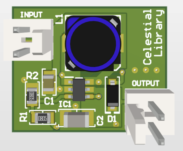
Finally, the 3D design of the finished compact DC-DC boost converter:
Conclusion
The design of a boost converter is a new step in these electronics design lessons. Many devices, especially portable and battery-powered ones, use a boost converter to raise the supply voltage to the level required for the supply to the integrated circuits. Most of the ICs cannot maintain their operations while supplied with just 1.5 V or 3 V.
At first sight, it may seem that this is a relatively simple design, but there are still some factors the designer needs to consider. The market gives the designer the ability to choose from thousands of different boost converters, so choosing the right one may not be straightforward.
As you can see, the boost converter topology is also quite different from the buck converter. The PCB design will also be different. However, fundamentally the considerations are the same; the designer needs to try to make the input and output current loops as short as possible to reduce any EMI radiated from the supply.
As there are many more different switching regulator topologies possible, this one will be the next step in power supply design.
You can find the design files for many of my projects released under the open-source MIT license on GitHub. You’re free to use any of the circuits or projects as you wish, even for commercial projects. You’ll find details of the devices that we discuss in my massive open-source Altium Designer Library®. You’ll also find details of a huge range of different components contained in this library as well.