How to Calculate PCB Power Plane Current Capacity

Power planes are an integral part of your PCB, but how large should they be, and what current can a large plane comfortably carry? The truth is a designer has some flexibility to adjust their constraints to accommodate larger currents in their PCB power planes, but the power plane size will limit the maximum PCB power plane current capacity. When you need to ensure high reliability, the IPC standards are a good place to start sizing your power plane to ensure your board stays cool.
Understanding PCB Power Plane Current Capacity
Power and ground planes serve multiple purposes in your PCB beyond just carrying current to and from components. They’re an integral part of DC and AC power integrity, and they often require the same attention to detail as the rest of your PCB layout.
Since all conductors have some DC resistance, they will dissipate some power as heat when they carry some current. Just like any other conductor, the size of a copper plane will determine its DC resistance, which will determine how much power is dissipated as heat in the power plane. Just like when trying to determine minimum trace widths, there is a minimum power plane size for a given required DC current, or a maximum PCB power plane current capacity for a given plane size.
Why Use Large Planes?
From the perspective of DC resistance and power dissipation, there are two reasons to use larger power planes:
- Lower DC resistance: Physically larger power planes can be made wider and will have lower DC resistance than a narrow plane, so they dissipate less heat.
- Larger heat transfer: Power planes in a PCB can transfer more heat away from hot components compared to the bare substrate.
For AC and EMI reasons, physically larger planes are also desirable as they provide greater interplane capacitance for decoupling in high speed boards, and they provide some isolation to EMI. However, since the primary job of a PCB power plane in many power systems is to carry high current around the board, the first place to start designing is to determine the maximum current your plane can carry without getting too hot.
Power Plane Current Capacity Calculation
The best place to start calculating your power plane current capacity is to use the IPC 2221 standard. For high voltage designs, this standard covers multiple design reliability aspects but is said to be less conservative than the related IPC 2152 standard. This calculation will tell you the temperature rise you can expect for a given plane size and current, or it can be used to determine the plane size for a given temperature and current. Most calculators you’ll find on the internet will take the latter approach. The inputs into this calculation are:
- The maximum allowed temperature rise from the external ambient temperature (10-20 °C is a common choice)
- The copper weight of the power plane
- The required current (in Amps)
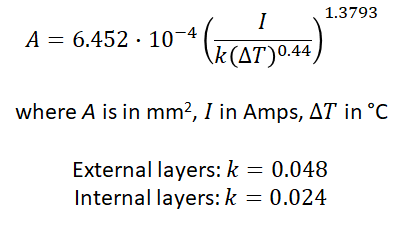
First, calculate the minimum required area using your desired current and temperature rise values:

Next, calculate the cross-sectional width of the plane from the area using the copper weight. The thickness of a copper plane with 1 oz./sq. ft. weight is 0.35 mm, so you can use this to calculate the span of your plane. The best design tools will help you evaluate your results with a post-layout simulator to spot areas where current and temperature are too high.
If you like, you can switch this around to get a current limit for your allowed temperature rise. First, you’ll need to solve the above equation for the current. Next, take the cross-sectional area of your plane and your specified temperature rise, and plug these into your solved equation. You now have the maximum current limit for your power plane.
Designing for Higher Temperatures or Currents
If you need extreme heat dissipation away from your board, such as in a power system or an automotive system, a ceramic or metal-core substrate are some options. These substrates will dissipate more heat away from the board, so you can expect your system to sit at a lower steady-state temperature during operation. You might be able to remove a cooling fan or heatsink from the system, depending on where the board will be deployed.
Another simple option is to just use multiple power planes on multiple layers. As an example from a recent project of mine, we did a 6U backplane that needed to carry up to 100 A from a pair of hot-swappable power supplies to multiple daughterboards on different connectors. Such a board is already pretty large, but the plane sections in one area of the board could only carry ~20 A without increasing the board’s temperature to an unacceptable level. The solution? Use multiple power planes on different layers! Running power planes in parallel is equivalent to using thicker copper and will increase your total PCB power plane current capacity.
A similar example is shown below, where two power planes at different voltages are used to carry high current. The low voltage/low current plane is shown in burgundy, and the high voltage/high current plane is shown in green. If you’re creative with your power distribution design, you can split currents between different planes to help keep the temperature of any single plane from getting to high.

Once you’ve determined the power plane current capacity, you can examine the DC current distribution in a DC simulation with a PDNA tool. Mark Harris provides two great tutorials in these articles:
- Copper Current Density for Simulations, The Quick and Dirty Way
- PDN Analyzer Quick Start on a Motor Driver PCB
If you’re designing power electronics and you want to ensure reliability in your next system, use the complete set of PCB design and layout tools in Altium Designer® for your next design. The upgraded Design Rules Editor in the newest version of Altium Designer lets you define IPC standards as your design rules and helps you create a manufacturable layout. You can also use the high voltage design tools and PDN Analyzer extension to make sure you haven’t exceeded your PCB power plane current capacity as you create your PCB layout.
When you’ve finished your design, and you want to share your project, the Altium 365™ platform makes it easy to collaborate with other designers. We have only scratched the surface of what is possible to do with Altium Designer on Altium 365. You can check the product page for a more in-depth feature description or one of the On-Demand Webinars.
