High Speed Backplane Design and PCB Layout Tips

If you need to connect multiple boards into a larger system and provide interconnections between them, you’ll likely use a backplane to arrange these boards. Backplanes are advanced boards that borrow some elements from high speed design, mechanical design, high voltage/high current design, and even RF design. These boards are often used in mission-critical defense systems, telecom systems, and data centers. They carry their own set of standards that go beyond the reliability requirements in IPC.
Although backplanes follow particular standards not seen in many other PCBs, the concepts involved in layout and routing are familiar to many PCB designers. A large number of connectors and nets, and the tight space on a typical backplane, can appear challenging at first. Still, some simple strategies can help you stay organized and complete a backplane design while ensuring high reliability. My hope is that you’ll learn some strategies to approach your next backplane design in terms of routing and layout to balance reliability and signal integrity. Without much more, let’s jump into this rich area of PCB design.
Getting Started with Backplane Design
There are multiple angles to take when getting started with backplane design, layout, and routing. These designs can be difficult because you might find yourself managing thousands of connections across a large board with limited space and layer count. Furthermore, backplanes might be involved in actually supplying power to daughtercards, and each daughtercard might be pulling multiple Amps of current through a variety of high speed devices. This means your backplane might need to support ~100 A of current.
Since a backplane’s primary function is to provide connections between multiple boards in a larger system, everything revolves around the connectors you’ll use, and these connectors are where your design begins. Here are some of the basic tasks involved in backplane design:
- Pinout: The first step is determining the pinout on your connectors to support your required routing topology. I’ll get into this point more below.
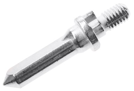
- Mechanical requirements: In addition to proper placement of daughterboard connectors, guide pins are used to ensure proper mating and structural integrity. The image at the bottom of this list shows a typical guide pin used with backplane connectors.
- Material selection: For high speed backplanes, this is a critical point in the design process. As backplanes can be quite large, any signal that needs to travel across the entire plane could experience significant loss. Low-loss laminates with tight glass weave are needed to help minimize insertion loss on long interconnects. Some examples that are useful for multi-gig backplanes are Rogers and Megtron laminates.
- Power and grounding strategy: For backplanes that need to carry high power to a large number of daughterboards, you’ll need a power and grounding strategy that helps keep temperature low. The ground/power plane arrangement on different plane layers should also provide isolation for high speed signals being routed around the board.
- Layer count: The number of layers you need in your backplane will depend on the plane layer count as well as the number of signal layers you’ll need. A backplane could have up to 24 layers and be several mm thick to accommodate all design requirements.

The points above are the same points you would need to consider in any other high speed design. However, things get a bit different once you’re working on a backplane as your connector pinout will constrain routing. This is a big part of backplane design and should be planned carefully.
It’s All About Connectors, Pinout, and Routing
Much of the focus in the initial design stages will be on the connectors in your backplane. Connector selection, including for backplane connectors, is as much an art as it is a science, and these connectors will be major determinants of signal integrity. Simulations are quite important for ensuring signals do not excessively degrade at connector-trace interfaces.
The pinout in your connectors is also critical as it will aid ease of routing on each layer. In particular, your pinout should accomplish two objectives:
- It should be designed to prevent signals on a given layer from crossing each other as signals are routed to all connectors on the backplane bus. If done properly, you can probably eliminate a few signal layers.
- Ideally, routing should be fluid across the entire backplane (everything largely horizontal) as pins on each connector are reached.
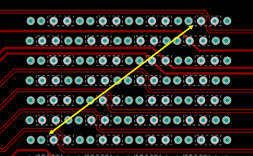
Things are best done in a row-by-row manner, similar to the differential pair routing I’ve shown below. Note how the pins on each connector are staggered in each column, which allows traces in the differential pair to come between rows of connector pins. If all pins were in the same column, I’d need 2 layers to do the routing shown below instead of 1.

Given all these design requirements, I found it difficult to balance them all in my first backplane, and we didn’t even do the initial component arrangement. You won’t have a lot of freedom in terms of component arrangement, but you can keep things organized as you route signals through the backplane as long as your pinout is organized and consistent across your connectors. Some other tips to help you be successful include:
- Minimize via transitions on high speed signals. Each via adds insertion loss to an interconnect, and insertion loss needs to be minimized as much as possible.
- Backdrill high speed via transitions. Backdrilling adds cost, but it minimizes stub discontinuities on long transmission lines.
- Don’t be afraid of ground pour. Using ground pour aids isolation between different groups of high speed traces, ensures consistent impedance profiles, and helps provide plenty of conductor for high return currents.
- Make all unused signal layers into plane layers. If you’re providing power through your backplane, don’t be afraid to throw an extra power plane into the layer stack. Splitting current between multiple power planes helps keep your PDN cool.
Backplane design is not for the faint of heart as it requires multiple specialties for success. However, if you have the right team of designers and a complete set of design tools, you can get through most aspects of the design process in a single platform. Altium Designer® is the only program that gives you a full suite of design tools for layout, routing, signal integrity, manufacturing, and much more. You’ll be able to complete your backplane design and prepare it for production in a single program.
Once you’re ready to push a completed backplane design out for manufacturing, you can share your design data on the Altium 365® platform. We have only scratched the surface of what is possible to do with Altium Designer on Altium 365. You can check the product page for a more in-depth feature description or one of the On-Demand Webinars.
