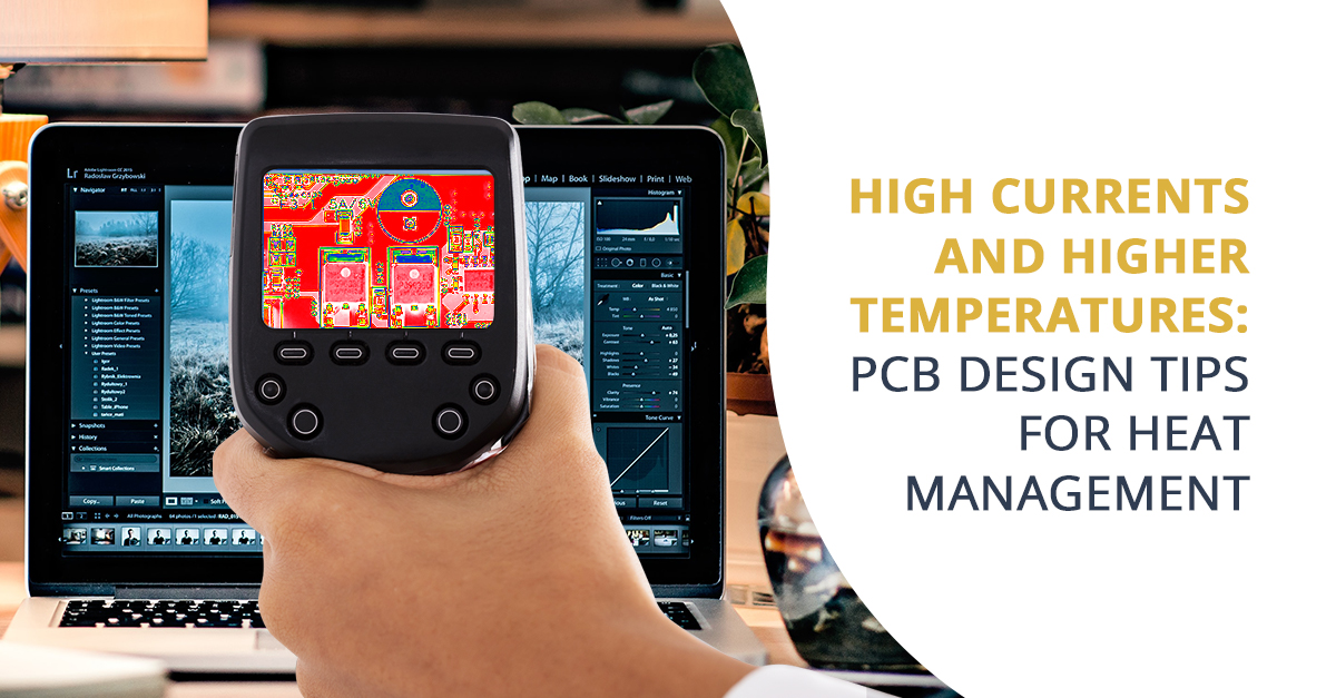
High Currents and Higher Temperatures: PCB Design Tips for Heat Management

I remember the first (and hopefully the only) time one of my circuits caught on fire. It started with the resistors and quickly spread to a nearby decoupling capacitor. Thankfully, the destruction was minor and most of the components were salvageable. Why did this happen you ask? No, this was not due to a short circuit. Very simply, I did not take into account the high current PCB layout.
As electronics continue to be miniaturized, the thermal demands in these systems increase as more features are packed into smaller devices. This is especially true in printed circuit boards (PCBs) that operate at high current-carrying capacity. Power systems with high output, such as Li+ ion batteries used in electric vehicles, require integrated power management systems that are built on PCBs. Designers will need to implement creative strategies to manage heat generated in a high current PCB layout.
Heat that is generated by power loss in high current circuits should be moved away from the device in order to combat temperature rise. Everyone is probably familiar with fans and heat sinks used on computer processors. These systems essentially move heat from the board and exchange it with moving air. But in some PCB devices, especially devices with small form factor, incorporating a fan or a bulky heat sink may not be possible on the ground plane. Read on for some high current PCB design tips.
Heavier Copper for Higher Currents: PCB Design Tips
The resistance of copper traces and vias account for significant power loss and heat generation in PCB-based devices, especially when they carry high current density. Electrical connections with a larger cross-sectional area have lower resistance, which reduces the amount of power lost to heat.
The amount of copper used in most PCBs is equivalent to about 1 oz. per square foot. When using free pcb software and integrating fans or heat sinks is not possible, a PCB with high current density should use at least double this amount of copper. Circuits operating at over 10 amps should go as high as 3 or 4 oz. per square foot.
Using a large amount of copper will require that the trace width on the PCB be increased. To keep from losing usable area, the PCB trace can be placed deeper into the board. This will also help dissipate heat into the board itself and into any nearby thermal vias. Of course, this will likely require the use of a thicker board, which can be desirable in high current devices.
Thermal Vias and Landings
Heat cannot be efficiently exchanged with stagnant air around a hot device. But heat can be transferred away from the critical electrical components in the board using thermal vias. A thermal via is a good conductor of heat that runs between the top and bottom of the board. Heat is transferred to a thermal via by simple conduction, and the thermal via allows heat to move away from the critical electronic components.
A thermal landing is basically a metal plate mounted on the bottom of the board. After thermal vias transport heat away from the hottest spots on the board itself, it must go somewhere else to maintain heat dissipation from hot spots on top of the board. The thermal vias transport heat to the thermal landing. Ideally, the thermal landing should be located in a portion of the board that is not a point of failure.

Placing High Power Components
High current electronic components like microcontrollers can generate a significant amount of heat. It is a good idea to mount these components near the center of the board when laying out your printed circuit board design. This is especially true for semiconductor components that use a PowerPAD style package.
If a component is mounted near the edge of the board, the heat it generates will accumulate and the local temperature can be very high. But if the component is mounted in the middle of the board, heat can diffuse throughout the board, and the temperature of the board will be lower.
Multiple high power PCB components should be distributed throughout the board rather than clustered in a single location. It may even be preferable to separate the components among different boards, as long as the form factor of the device can accommodate this. Always be mindful of component placement as it can have a major impact on your manufacturing budget.
Thicker Boards
The life of the electrical connections, components, and the board itself will be shortened when the device runs at extreme temperatures. The computer hardware industry has reduced this problem using cooling fans. But when a fan is not used for cooling, most of the heat is thermally conductive, directly into the board and the surrounding components. If the board thickness is very thin, everything can heat up to a high temperature.
A thicker board will require more thermal energy to heat up to a high temperature. This helps keep the temperature at the top of the board low. If the board is mounted directly to the packaging, heat can be conducted to the exterior of the device. The trade-off with this solution is that the production costs will be higher.
The best heat dissipation strategies to use will depend on a number of factors. Not all designs or form factors can accommodate all the strategies outlined above. For example, thermal landings are not suitable for double-sided PCBs. If a large number of components are present on the board, some of them will inevitably get placed near the edge of the board.
The Altium Designer® software package has advanced functionality that can allow you to visualize potential hot spots in your PCB. The PDN Analyzer™ tool allows designers to identify trouble areas that can lead to failure in high current devices. Talk to an expert at Altium Designer to learn more.