Ground Bounce Reduction Techniques to Minimize Signal Integrity Issues

Unlike my dad who thrived on the basketball team during his school days, I could barely bounce the ball during tryouts. Needless to say, I quit sports before I even started. While my dreams of becoming an NBA pro were dashed, I later discovered my passion for martial arts. I never really got into handling a basketball well, but in martial arts at least I could bounce off the balls of my feet to meet my opponent.
Not being able to bounce the basketball is one thing. Not understanding ground bounce in electronics, however, can be very problematic for your circuits. To excel as a solid PCB layout engineer, being knowledgeable about the effects of ground bounce on circuits and signal integrity is necessary. By taking ground bounce reduction techniques into consideration, you can minimize ground bounce in PCB signal integrity across your designs.
What is Ground Bounce?
To understand ground bounce, you need to dive into the basics of a sleep transistor and ground pins that form the core of integrated circuits (IC). The image below shows the Complementary metal–oxide–semiconductor (CMOS) circuitry of ICs like microcontrollers and random access memory (RAM).
Ground bounce noise in a PCB is a difficult problem to measure, and the effects it has on power gating and signal integrity are related to the trace impedance and PDN impedance in a PCB. In most high speed designs, the output pin of a driver circuit is usually connected to a load with some input capacitance. When the output pin is asserted to logic circuit ‘1’, the parasitic capacitance at the load is fully charged to VCC. As the output buffer circuit is turned off to logic ‘0’, the capacitive load discharges to provide the inrush of current back to the driver; this quick rush of current flows through the driver's ground pin.
In an ideal situation, the ground of the IC package and the board will remain at the same voltage. In a realistic design, however, some parasitic inductance is present between the die-ground and the board ground due to the bond wire, lead frame, and parasitic inductance in the PDN. The total package inductance from these elements can be modeled as a set of inductors in series, as shown in the above schematic.
As the current rushes through the inductance on the bond wire/lead frame/PDN, a back EMF builds up between the die-ground and the board ground. This causes a phenomenon where the die-ground and the board ground are at different voltage levels for a momentary period, which results in ground bouncing noise. This buildup is then damped due to the DC resistance of these elements and parasitics in the IC package/die. To better understand exactly how this affects signal behavior, it helps to understand that this arrangement of parasitics and the trace form an equivalent RLC circuit with some defined impedance and resonance frequency.

How Ground Bounce in a PCB Affects Circuits and Signals
When ground bounce in a PCB is minimal, it may not cause any disruption to the die ground or signal behavior. It will still occur, but it might be small enough as to go un-noticed. However, when back EMF produced by ground bounce is large, especially when multiple outputs are switched simultaneously, the ground level of the device rises to a level that may affect other groups of pins on the IC.
When you look at the trace connecting the driving component to the capacitive load, the trace inductance and capacitance also influence how ground bounce affects your signals. Remember that all traces have some impedance due to their parasitic capacitance and inductance. Because a real trace has these parasitics, they need to be included in the lumped RLC network formed by the trace, inductances at the driver's ground pin, and the load capacitance.
Level Shifts on the Die
As an example, a microcontroller experiencing ground bounce may have its ground potential shifted such that the voltage measured between the power rail and ground is 1.5 V higher than the case without ground bounce. In other words, the potential difference between the power rail and the die ground would be 1.5 V higher than the potential measured between the power rail and board ground. Another way to state this is that there is a momentary 1.5 V potential between the die ground and PCB ground plane (i.e., measured across the driver's ground pin).
In this example, a logic IC operating at 3.3 V that is connected to the microcontroller may interpret a logic ‘0’ signal as a ‘1’ because it is receiving a 1.5 V logic ‘low’ signal due to the shifted potential level of the device ground. To continue with this example, a device that is experiencing a ground bounce could also misread inputs from other components because the input voltage level is seen with respect to the die ground. For example, a logic ‘high’ signal might be misinterpreted as ‘low’ because the voltage at the input pin is 1.8 V instead of 3.3 V, due to the rise in the die ground. This is below the minimum logic high voltage of 2.31 V.
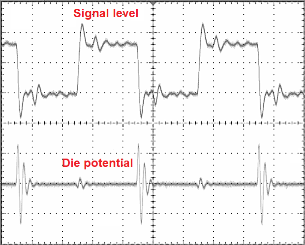
The effect of ground bounce is at its worst when all outputs are simultaneously driven low (see the above image). That’s when the voltage difference of the die-ground increases drastically. In addition, this level shift acts like a fast-rising signal in an RLC network, which can exhibit an underdamped transient oscillation in certain conditions.
Oscillations in a Level Shift
The level shift on the die ground does not persist forever, and the potential difference between the die ground and the PCB ground eventually falls back to zero. Because the trace and load provide some parasitic capacitance, this level shift can exhibit a damped oscillation, just like you would observe in an RLC circuit. That these oscillations can exhibit various levels of damping depending on the total resistance in the current loop. If there is an oscillation in the die ground, this oscillation will be superimposed on an output signal, creating a transient ringing phenomenon. The image below shows such an underdamped transient oscillation due to ground bounce.

In an imperfect situation, the driver's output impedance is zero and the load input impedance is infinity, and any transient generated on the trace will have zero damping. In a real situation, the damping will be non-zero due to DC conductance through the driver and its impedance in the LOW and HIGH states. The damping is equal to (R/2L), where R is the total resistance around the sinking current loop and L is the lumped equivalent inductance of the circuit containing the sinking current.
If the trace inductance is low enough, the damping constant will be large and any ground bounce oscillation will damp quickly. If the lumped trace inductance is low enough and the lumped capacitance is large enough, the transient due to ground bounce can be overdamped. This is one of many reasons DDR channels opt for slightly lower trace impedance (40 Ohms single-ended impedance) as they will have lower inductance. Capacitive loads with higher input capacitance will have larger damping, which becomes problematic in high speed PCB design: components with faster edge rates tend to have lower input capacitance and more problems with ground bounce.
Tips to Reduce Ground Bounce in a PCB
The easiest way to reduce the effects of ground bounce in a PCB is to place a bypass capacitor close to the affected component. Physically, the bypass capacitor acts like a battery that compensates a change in the die ground potential as measured with respect to the power rail. The bypass capacitor also accepts some current from the discharging load capacitance when the driver switches. It is important to place the bypass capacitor as close to the VCC pin of the component as possible to minimize the total inductance of the ground trace. It is also appropriate to place the capacitor to a pad connected to the ground plane through two vias, which will provide a lower inductance path to the PCB ground plane.
Placing a resistor in series with the output load is also a standard strategy used with low impedance drivers. If your traces are long enough to act like transmission lines, you'll likely need to do this anyway to provide impedance matching at the source end. This will increase the damping constant seen by the output signal from the driver, which slows down the transient rise time of the changing signal and can bring the transient oscillation into the overdamped regime. This is only applicable when the output is not timing-sensitive, such as an address bus for a parallel SRAM.
As a general rule, you should avoid placing glitch-sensitive signals such as RESET, CHIP SELECT, or SET on the same logic IC that is prone to ground bounce issues. Overall, output pins that are closer to the GND pin experience smaller level shifts and weaker oscillations due to ground bounce.
Design Your Board to Have Low Ground Bounce
Ultimately, placing bypass capacitors and properly designing trace widths are effective methods that are applicable to a broad range of designs. When done correctly, you can ensure impedance matching and signal integrity simultaneously. A low impedance PDN also reduces ground bounce and other power integrity problems that occur in high speed PCB design. To minimize uncontrolled voltage drops across your designs and uncover other potential power dissipation issues, try using Altium Designer to accurately design your PCB.
Altium Designer on Altium 365 delivers an unprecedented amount of integration to the electronics industry until now relegated to the world of software development, allowing designers to work from home and reach unprecedented levels of efficiency.
We have only scratched the surface of what is possible to do with Altium Designer on Altium 365. You can check the product page for a more in-depth feature description or one of the On-Demand Webinars.