Expert Analysis of Measured S-Parameters
Introduction
There are many tutorials on S-parameter analysis. The topics usually include how to identify port maps, what insertion loss and return loss looks like, and how the various S-parameters look in the time-domain. For beginners, this is quite valuable. Here, we will briefly explain those topics and add some additional analysis techniques to use when data mining S-parameters.
Brief Overview of S-Parameters
S-parameters are basically transfer functions. You can multiply a stimulus in the frequency domain, like a pulse, by the S-parameters and you get the response of that pulse after it has gone through the channel represented by the S-parameters. The channel could be a passive channel like a cable or an active channel like a CTLE.

So, the basic idea is S-parameters are used to get an understanding of what is going to happen to your signal after you put it through this black box. In two-port S-parameters, S21 and S12 are insertion loss or transmission parameters, and they should be approximately the same. S11 and S22 are the return loss or reflection parameters. These can be unique if the device is not symmetrical. These are typically plotted in voltage dB.
Where, A is your input S-parameter: S21, S11, ect.
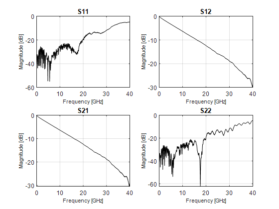
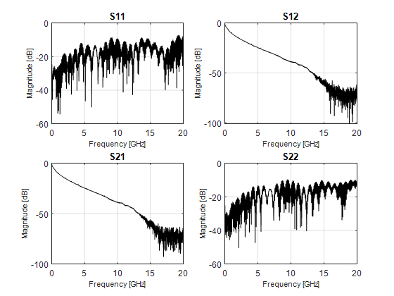
In this example, S21 and S12 are practically identical. S11 and S22 have some significant differences like the large resonance in S22 around 18 GHz that is absent in S11.
Here is where I’d like to shine my first bit of extra knowledge to you. Don’t just look at the S-parameters in decibels; look at the phase. Calculate phase with:
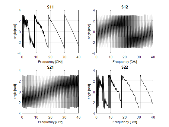
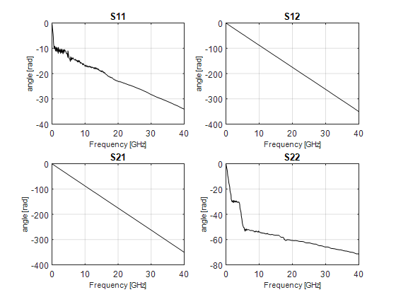
You will also need to unwrap the phase. Unwrapping the phase simply means to add or subtract 2 x PI every time the phase shifts by 2 x PI, so the phase looks like a straight line. The plot below on the left is wrapped, and the right is unwrapped.
 |
 |
|---|
Phase can answer a few questions:
- Is there enough data to take this into the time-domain?
- Is this data valid across the entire measured frequency band?
- What is the delay of this structure?
Let’s take these one-at-a-time.
Is there enough data to take this into the time-domain?
To answer all these questions, we’ll look at the transmission parameter, S21. The phase should be monotonically moving at a negative slope from DC to the highest available frequency. That means there is more than one point between shifts from -pi to pi before unwrapping. If there is one point or less between shifts, something called aliasing occurs when you perform the conversion from frequency to time. When these S-parameters are converted into the time-domain, the data looks shorter than usual or even non-causal (information before t=0). The time-domain information is basically unusable in these scenarios. In these cases, unwrapped phase has a positive slope from DC to the highest frequency, and I have an example of this below in figure x. To fix this problem, measure the S-parameters with a smaller frequency step. In general, a 10 MHz step S-parameter will never have this problem.
_6.png)
Is this data valid across the entire measured frequency band?
Let’s take a look at some measured data to answer this question.
 |
 |
|---|
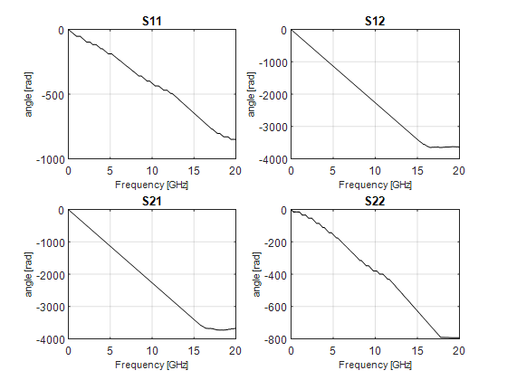
The data on the left is in decibels, and the right is the unwrapped phase. You can see in the insertion loss, the data gets fuzzy around 15 GHz, but the return loss looks OK. If you look at the phase, it starts by having a negative slope, which is good. Then at around 16 GHz, you can see the slope becomes zero. This is because the S-parameters are at the noise floor of the VNA, and the VNA can no longer acquire the phase. When the slope becomes 0 like this, the S-parameters are invalid. It is not always possible to fix this. VNA’s have a noise floor of about 80 to 110 dB depending on the IF bandwidth setting (lower IF bandwidth, lower noise floor). Time-domain VNAs have a noise floor closer to -40dB.
What is the Delay of the Structure?
Signal integrity engineers usually measure the delay in the time-domain with a step response. They measure the 50% crossing of the input step from a TDR. Then they measure the 50% crossing of the output which has passed through the device under test. There are popular modifications to this method, such as taking the derivative of the step responses and measuring the delay of each peak instead of the 50% crossing. There is also the method of measuring the crossing at a fixed voltage instead of the step’s relative amplitude. Finally, you could also measure at a different crossing, such as the 5% point.
All these are good, but there are a few things that can be better. First is the idea of using different test equipment for the delay measurement. It would be better if only one were needed, and since we know the VNA has a lower noise floor, the VNA is the obvious measurement device of choice. Second is lab-to-lab consistency. VNA’s are easily capable of NIST traceable reference planes with a Short-Open-Load and Unknown-Thru calibration. The calibration of the TDR is not NIST traceable, and this makes lab-to-lab correlation quite difficult. Finally, there is data transfer. Time-domain digital data does not have a standard format and is usually shared with an Excel spreadsheet. VNA data has many standard formats which include the ubiquitous touchstone file. Practicality all EDA tools accept a touchstone file, and having this format available makes communication much easier. So, let’s use a VNA and figure out how to get a delay from there.
The first method is to do the same thing the TDR does with a frequency-to-time conversion. There are a few advantages to this. First, you can integrate the transfer function to get the step response. This way, there is no need to measure the input step first, and you only have one delay to measure instead of two. The argument against this approach is there will be fewer points available from the frequency-to-time conversion, and you will have too much uncertainty. This is a reasonable point, but the slope of the step response through a channel is so consistent that it is quite simple to interpolate to the nearest picosecond. The slope of the step does not vary much, and it is quite simple to get accurate interpolated data.
| Step Response | Zoomed |
|---|---|
_4.png) |
_2.png) |
Red is the raw data, and Blue is interpolated with the spline method. The data cursors are the discrete points around the 50% crossing from the raw data.
You may say, “Yeah, that’s great, but I don’t know how to do a frequency-to-time conversion or interpolate.” Well, this is where the VNA is even better because you don’t need to. If we look to the phase again, we can apply a simple formula to get the delay.

What’s great about this equation is you get the delay in nanoseconds by simply dividing by frequency in gigahertz.
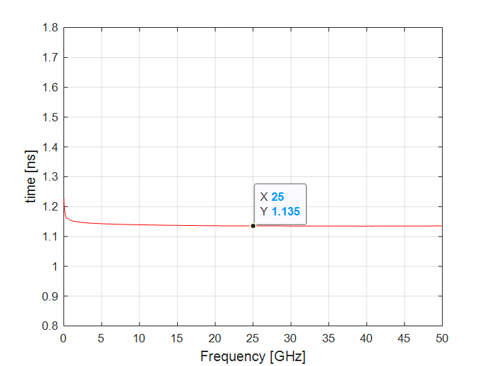
First, notice I plotted the y-axis on the same scale as the x-axis in the step response plot. In the step response, the delay isn’t nearly as consistent as in the frequency domain method. From 10 GHz to 50 GHz, the delay is basically the same. That makes this method very consistent between labs. The next thing to notice is the delay at 25 GHz, as shown, is a little different than that of the step response. That’s because the 50% delay is found somewhere at the low frequencies of this plot where the phase changes quickly with each point. This is again another reason why the step response method is somewhat unreliable for lab-to-lab correlation. I also like that you can pick a frequency point to use instead of a crossing, which is much less ambiguous, and there is no need for interpolation.
Calculating Skew Quickly and Easily
When debugging channels, skew is one of the first things to check. Skew is the delay difference in the positive and negative sides of a differential transmission line. When transmission lines are loosely coupled, this trick can allow you to calculate skew very fast. First, convert the single-ended S-parameters to mode-conversion. Another way to say it is S to SCD. Then plot the SCD21 data in dB and find the first minimum.
_13.png)
Take the inverse of the frequency and that is the skew! Let’s see how this lines up to the delay method discussed earlier.
Delay of line 1: 1.38482356955646ns
Delay of line 2: 1.42117027815264ns
Difference in delays (skew): 0.0363467085961828ns
Skew calculated from SCD21: 1/27.52 = 0.0363372093023256ns
Error: 9.49929385720555e-06ns (pretty much zero)
This trick usually only works when the skew is relatively large (>50 ps).
What is the common-mode telling you?
Common-mode is an often neglected parameter. It comes up during electromagnetic interference (EMI) discussions to help find leaks within a transmission line. However, the common-mode can help you understand what you are looking at and how the structure works and where you can expect problems.
First, let’s look at common-mode in the frequency domain. Here, you want to compare common-mode insertion loss to differential insertion loss. This compares how well the signal return path is behaving compared to the signal only. If we look at a stripline differential pair in this way, you can see the common-mode and differential mode behave similarly. I would expect this type of behavior in the twin-axial cable as well.
_10.png)
When an interconnect is placed into the channel, things start to look different. The common-mode begins to deviate from the insertion loss. In this case, it is near 20 GHz, and I would expect to see increased radiation or crosstalk at frequencies where this deviation is present.
_7.png)
Another place to look is in impedance. Common-mode impedance is referenced to 25 ohms. When the impedance is lower than 25 ohms, the signal is likely completely uncoupled, and the differential transmission line impedance is lower than 100 ohms. This is a fairly typical scenario in systems because many integrators like to use “loosely coupled” differential pairs to help with skew mitigation. When the impedance is high, the coupling within the pair has increased. It could also indicate where the ground is beginning to be starved. Impedances between 25 ohms and 28 ohms can be expected in coupled striplines (see the figure below) and can be as high as 32 ohms in twin axial cables. Interconnect common-mode impedances can be relatively high. QSFP connectors, for example, have been known to have common-mode impedance near 50 ohms. This isn’t a problem for most systems, and when doing analysis, knowing this behavior helps you understand where in the interconnect you are looking as you search for problems.
_5.png)
Would you like to find out more about how Altium can help you with your next PCB design? Talk to an expert at Altium.