Creating a Powerful 150W LED Driver for Driving Large Lighting Panels
Most of my recent projects have been working towards building a high CRI (Colour Rendering Index) light panel for cinematography. A good quality video light panel is expensive, and for good reason, but as a maker, I tend to like buying things instead of just buying them.
My goal was to build a 300-320W panel. However, I’ve come to realize that the limitation for a panel with that many LEDs is not driving them, but instead reflowing the board. A typical low cost DIY reflow setup with a converted toaster/pizza oven or skillet just can’t take a board that large. To be able to reflow the board, I’m building a vapour phase reflow oven which will have a maximum board size of 230mm by 180mm as another project. Because of this, I’ve decided to split the panel into two 150-160W panels instead. This should also provide me some additional versatility, as I can now separate the panels to offer more creative lighting options without drawing more power. I’m still planning to run everything from a 350W 48V power supply to have both panels powered from the same 48V source.
This project is available on GitHub for you to freely use as you wish. If you’re looking for the components used in the project, you can find them in my open-source Altium Designer Library.
Choosing a Driver IC
I want to use the Luminus Devices MP-3030-210H-40-95 for the light panels. It’s a white, high-power LED with a CRI of 95 and forward voltage of 6 volts. I want to use the highest voltage I can to reduce losses and keep the current as low as possible, thus reducing the heating on the LED panel. When looking for an AC-DC power supply in the 300-400 watt range, a 48V supply is the cheapest at the suppliers I use.
In a previous project, I tried to see how far a monolithic driver IC could go, and 65 watts was really pushing it, so for my final driver solution, I know I need a controller with external MOSFETs.
After considering many drivers, I settled on the Analog Devices LT3756EMSE-2. Not only does it look like it has great performance, it’s also a very good starting point for the design mentioned in one of the design references.
I looked at running the driver, which is capable of both buck and boost modes, in whichever mode offered the better performance. In buck mode, the driver needed 32 parallel strings of LEDs to reach the desired voltage, which meant I needed components with high current rating. Higher current rated components are more expensive than higher voltage rated components, so I am going to use the boost mode which I’d originally intended.
Calculating Component Values
The driver is rated for 100V output, therefore I’m aiming to run 16 LEDs in series, to reach 96V per string. This should give me a 1.8A load to drive.
Current Sense Resistors
The LT3756EMSE-2 has two current sense resistors to monitor the load.
The first resistor whose value I need to calculate is in series with the LED for programming the current through the LED. The LED controller detects the current drop across this resistor, which is placed on the high side of the LED string. The driver expects a 100mV drop across this resistor, and as I want to drive 1.8A in each string, a little application of Ohm’s Law tells me I need a 56 milliohm resistor.
The second sense resistor has a formula in the datasheet, and for boost resistors it is

When I substitute my values, this gives me a 20milliohm resistor.

This sense resistor is used to set the maximum switch current.
I’m going to use 2512 sized resistors for the design. They can more than handle the current and the large package will help dissipate heat, keeping my board cooler.
Voltage Dividers
The IC also has two voltage dividers of interest to us, the first is a typical undervoltage lockout divider to turn the driver off when the voltage on the pin falls below 1.22V. I’m setting this to 40V for this driver, as I want to allow some voltage sag when the driver switches on before the AC-DC regulator can catch up. The soft-start feature of the LT3756 should help reduce the voltage sag when switching on the panel, making sure voltage below my minimum set value is a definite sign of something not performing well on the regulator.
The second divider is the output voltage setting. For this one, I am aiming for 1.25V at the pin. I’m setting the divider for 96V which will ensure that the driver can’t exceed it’s 100V rating while still allowing the LEDs to be driven at full power.
Switching Frequency
There are a few considerations for switching frequency in this design, primarily component size, and heat from driving the gate on the MOSFETs. Lower switching frequencies will allow the driver to stay much cooler as it doesn’t need to provide as much power to the MOSFET if it’s not rapidly switching the gate on and off. A lower frequency will typically be more efficient, but will also need larger components. I’d like this design to be very efficient to reduce the amount of heat on the board, and also ensure I don’t need to move to a large AC-DC power supply to deal with an inefficient design. The LED panel will be quite large itself and PCBs are cheap, so I’m not overly worried about the size of the driver board for this application.
One final consideration is the duty cycle. If I want to make use of the 3000:1 resolution dimming which the driver is capable of, I will need a large margin over the minimum on-time of the driver, which a lower switching frequency will also provide.
Given how many factors are pushing me towards a low switching frequency, I looked at several inductor options and found the lowest switching frequency that was practical for inductor selection was about 250kHz. If I go any lower than this, I won’t be able to find suitable inductors at my regular suppliers.
Inductor
The inductor value is chosen hand in hand with the switching frequency. There’s a lot of iteration back and forth for selecting the two together to ensure the design is feasible to source parts for.
The datasheet has the following formula for the inductor value:

Which gives me

Admittedly, I did work this problem a little differently. I looked for the maximum value I could find for an inductor in a practical surface mount package to calculate the switching frequency. When I found out that frequency wasn’t going to work, I decided to put two inductors in series as the design reference was doing. This in turn allowed me to choose a 47uH inductor, which is close to perfect for a 250kHz design. I then verified the 250kHz frequency was going to be viable for the other design constraints set by the datasheet.
This leaves me with the huge Wurth WE-HCF 7443634700 inductor to meet the 5A minimum saturation current, while retaining a low DC resistance. Two of these 47uH inductors meet the inductance requirements perfectly, and the 8.5A saturation current is well above the minimum. With 12.2 milliohm of DC Resistance, they should not overheat. Not to mention, the large package will also provide a lot of thermal mass and also act somewhat like a heatsink.
Switching MOSFETs
According to the datasheet, our main concern for the power MOSFETs is going to be gate charge and drain to source voltage (VDSS). I also want a package that is relatively easy to deal with at DIY prototype quantities. Whilst the datasheet is not overly concerned with the RDS-ON resistance, I’m not sure how much copper area I’ll have for sinking heat, so I want to keep this low as well. Basically, I want to have it all without sacrifices!
There aren’t a huge number of MOSFETs that meet my requirements, so I’ve decided to go with the Infineon BSC060N10NS3GATMA1. Before I confirm the choice, I need to ensure the driver IC can deal with it, as the gate charge is perhaps the main downside of the MOSFET at 68nC. Luckily, I’ve chosen a low switching frequency which reduces the current required to drive the gate. I’ve also chosen to use the MSOP package instead of the QFN, as the MSOP has a thermal resistance (θJA) of 43°C/W which is more favorable when compared to the 68°C/W of the QFN.
We can calculate the junction temperature created by driving the FET with the formula in the datasheet. I’ve removed the ambient temperature parameter so we just see the actual temperature rise.

The driver can provide a maximum quiescent current of 1.5mA, so I will use that for the equation. With the other parameters already known, I get:

With the driver happy to operate at 125°C, this gives me a maximum ambient/board temperature of about 77°C. The driver will shut down at 165°C, allowing the board to reach about 117°C before we get to thermal shutdown. I wouldn’t expect to have an ambient temperature over 77°C, as there will be fans on the LED panel which will also cool the driver board.
High Power LED Driver Schematic
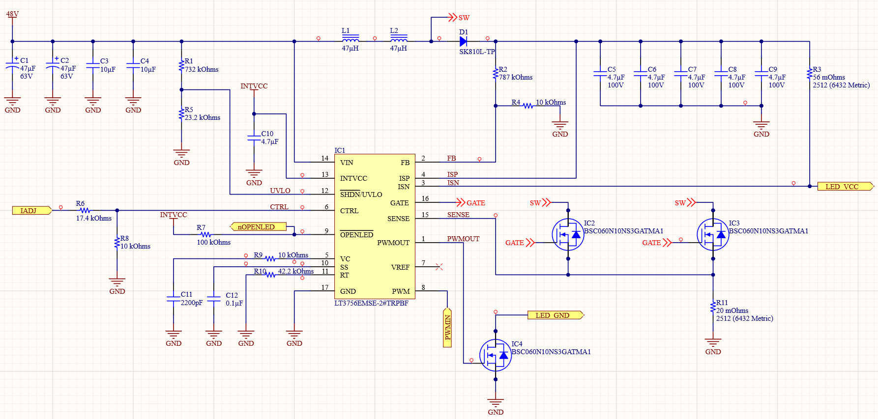
With all the values calculated, the schematic is very easy to draw out. The biggest challenge is just trying to make it legible and understandable.
Creepage and Clearance
As I’m dealing with 100V on the board, I wanted to add creepage and clearance rules for the board design to ensure things don’t go horribly wrong with the design from components or traces getting too close to each other at the high voltages.
If you’ve read any of my other projects, you’ll know I love online calculators. I’m using creepage.com for calculating the clearance and creepage requirements for the board. My calculated clearance is 0.5mm, and the creepage should be 1.4mm. Given the 0.195mm clearance between the MSOP package pins, this is more than I’d like, so I checked the ‘coated board’ option, which brings the creepage requirement down to just 0.2mm. Conformal coating is going to make it a lot easier to add to the areas of the board where I have less than 1.4mm creepage, than if I was designing the board for the large creepage requirements.
With the requirement for clearance and creepage, I’m adding a parameter set directive to each net in the schematic.
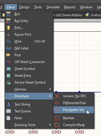
I’m using the Tiny style to keep the symbol small. The lower potential nets (such as ground), and the relatively low voltage nets, are getting a Net Class Name of ‘LP’, meanwhile the high voltage nets are getting added to a net class called ‘HV’.
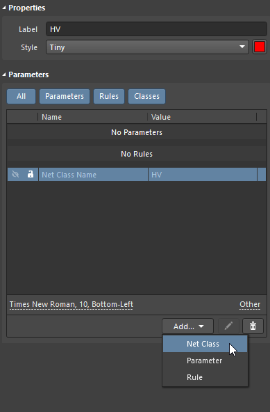
Once the parameter is placed, you can use the add button on the properties window to add a Net Class.
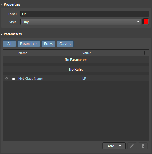
The same is repeated for the low potential nets.
Board Design
After adding all the components to my board, I attempt to figure out a rough layout for the components. For a design that is switching quite a lot of wattage, it’s critical to keep the current loop as small as possible to reduce EMI and ensure good operation of the driver.
This board will consist of four layers. Even though it’s a simple schematic, I do not want to cut up the bottom layer for logic traces to ensure a good thermal path for ground. The top layer will not be particularly effective for thermal purposes, as it will be broken into large polygons for carrying current. A 4-layer board does not come at a large additional cost over a 2-layer one, and will ensure we have a good thermal path. The top internal layer will also be solid ground, providing shielding from the high currents on the top layer from creating issues with the logic signals on the lower internal layer. In addition, this ground plane will also help shift some heat away from the driver IC.
After several layouts that were not really satisfying me, I settled on the rough layout below.
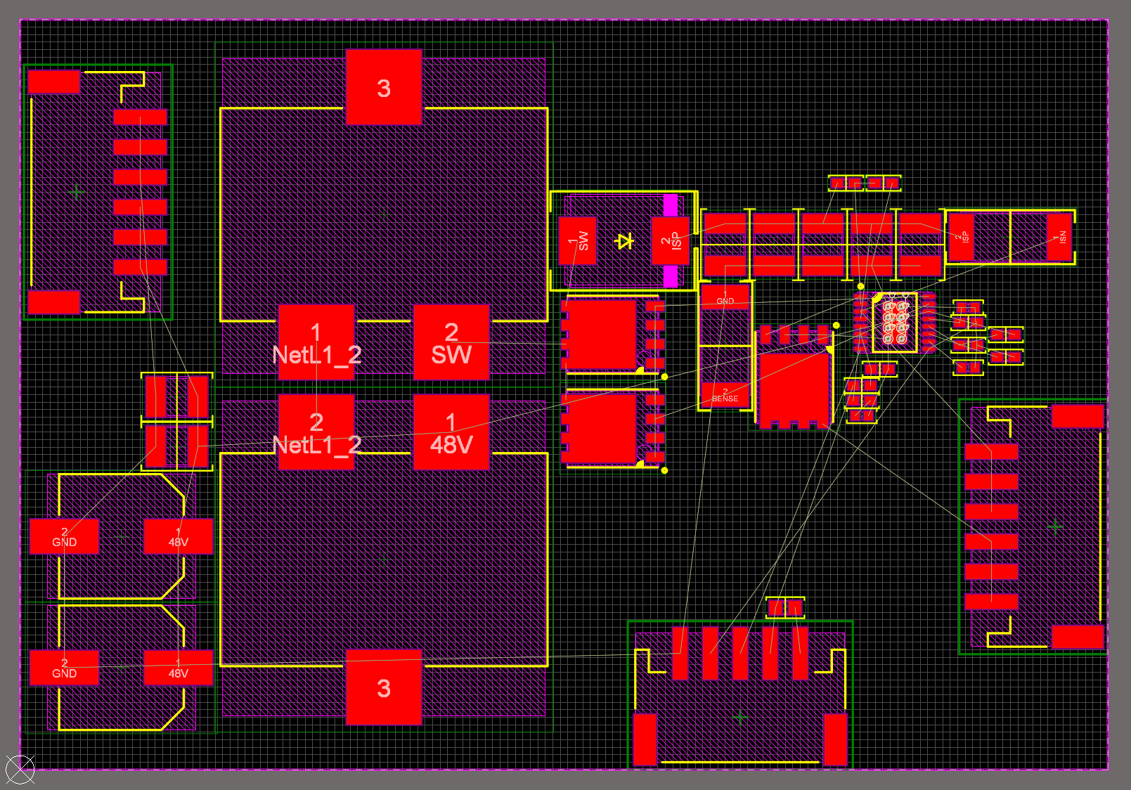
I’m not a huge fan of the input connector (top right) being so far from the regulator, so I’ll be adding a lot of vias around the ground connection to ensure there is a good return path. Before I get too committed to the layout, I need to set up the creepage and clearance rules for the high voltage nets.
I’m using JST PH connectors for power, as it is easy to find pre-crimped cables for them (JST KH series). The pins for the connectors are only rated for 1 amp, so to meet the demands of the circuit, I’m using 3 pins for ground and 3 pins for voltage. I had considered using something like bullet connectors soldered directly to the board, but the JST PH connectors are going to work well and will be a lot less hassle for assembly.
Creating Creepage and Clearance Rules
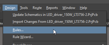
The first thing we’ll need is a new rule for the creepage distance. You can get to the rules by going to Design -> Rules.
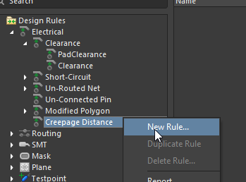
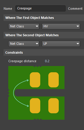
I’m adding a new creepage distance rule to the design.
In the properties of the new rule I can see my calculated creepage distance of 0.2mm (with conformal coating!). Typically you would expect the creepage rule to be much higher than the clearance rule.
Then we can do the same for clearance, with our calculated minimum distance of 0.5mm.
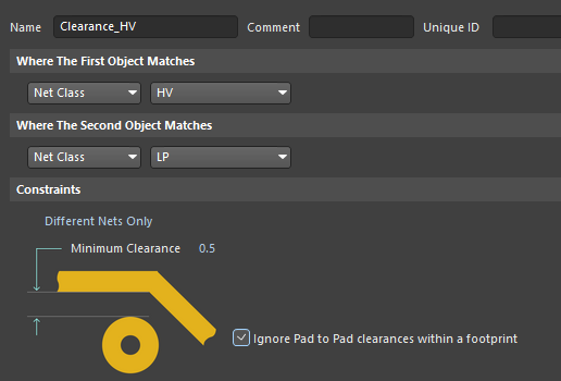
The problem with these rules is that any trace coming from the driver will violate the rule immediately as it is impossible to meet the clearance requirements.
I have a couple of options at this point:
- Create rules for each exception to clearly define what is allowed to violate the overall rule.
- Leave it as is, and check every design rule violation prior to signing off the design very carefully.
- Create a room for a local exception.
Using Rooms to Create Local Exceptions
I have to admit, I don’t use rooms as often as I should in my designs, if you’ve looked at my other projects, you may have noticed that I turn off room generation at a project level for most designs. However, creating localized exceptions to a rule is a case where rooms are really handy!
By default, a room automatically contains any object which is contained in the room. For most objects, this means the entire object must be within the room, however, for vias this means only the center of the via needs to be on or within the room boundary. I found this very handy later on in the layout process to restrict the room size.
To start off with, I’m going to add a new room. For my purposes here, I just need a rectangular room. The area I need an exception in is quite small and does not need complex geometry as a polygon would allow.
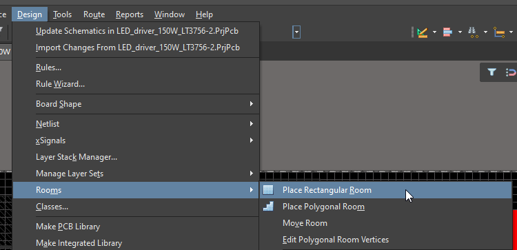
After placing the room and giving it the name ‘ClearanceException’, I then need to add a new clearance rule exception.
I could also add a new creepage rule here so I can just use conformal coating on the IC itself, and have an overall creepage requirement of 1.4mm for the board—however for this project I don’t feel I need to do that. You can use the same exact process as the exception for the clearance rule to create a creepage rule if you need to do this for your own projects.
I couldn’t remember the exact query to use for determining whether an object on the board is within a room or not, luckily the Query Helper window has it in the Membership Checks.
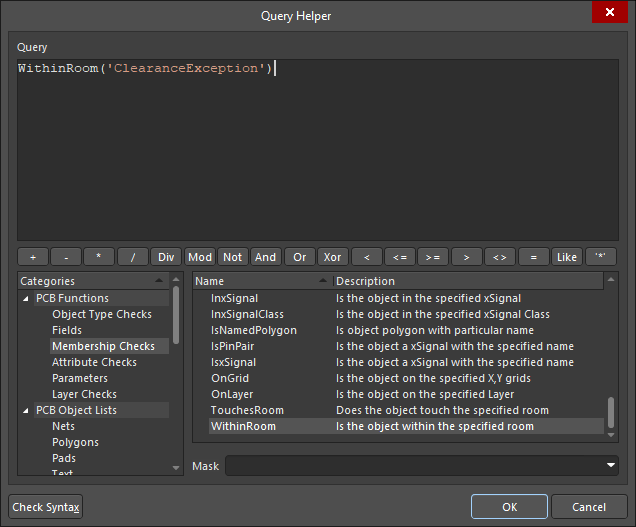
Our clearance exception then has a custom query for WithinRoom(‘ClearanceException’) and the InNetClass check.
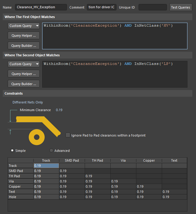
With this, I’m setting the clearance to 0.19mm. The pads on the footprint have a clearance of 0.195mm, so 0.19mm should make the design rule check happy.
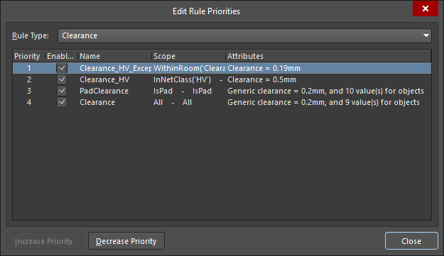
Finally, I need to ensure the rule priority is correct. Exceptions to a rule should always be first. The broader the scope of the rule, the further down the priority list it should be.
Looking back at my PCB with some initial routing work done, I can see my bright green violations are now gone.
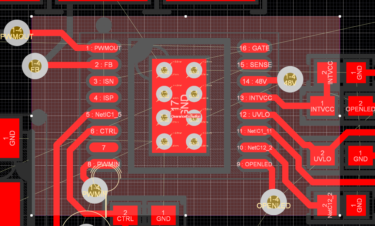
I’ll contract the room further as the layout progresses so it only covers the exact parts that need the exception applied to them.
Continuing the Layout
Now that I don’t have the horrible rule violations glaring at me, I can continue with my layout and routing. As usual with high power projects, I start out with ‘routing’ my board using polygons. I decided to go with rounded polygons for this board mostly for fun, but it does serve some purpose—for the higher voltage nets a hard corner is a place for a potential discharge if the solder mask is a bit thin or damaged. Given the quality of solder mask on even the cheapest boards, I have to admit that this ends up being a mostly aesthetic choice.
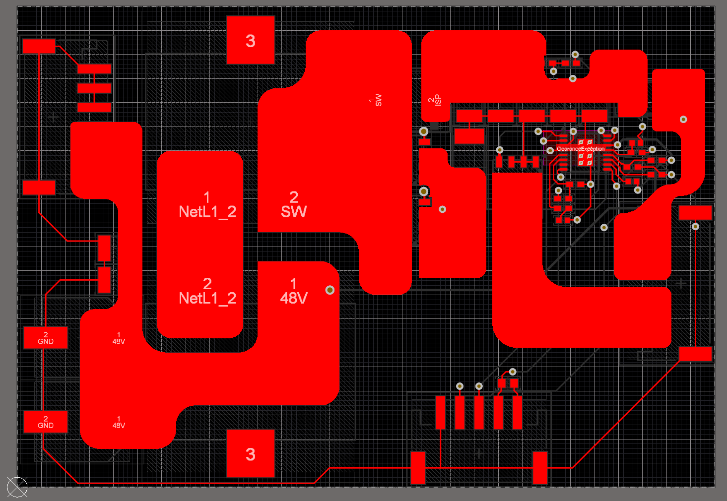
I’ve put the logic signal on the lower internal layer (mid-2) and tried to disrupt the bottom copper area as little as possible so it can be a nice big heatsink for the driver. I’ve tried to maximize the copper area of each top polygon that will be sinking heat as well.
My final layout has a lot of vias, many of which are likely overkill. I’m a big fan of overkill. There’s no ground pour in the top part of the board as it would serve no purpose. It’s not going to conduct much if any power, or act as a shield for any traces.
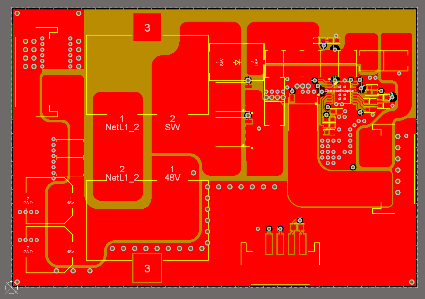
Power Simulation
In the past I’ve done separate articles on simulating the power distribution networks for this type of design, however, for this design, I just want to do a quick check so I’ll include it in this article. I’m only simulating the bare minimum, so my power network is quite simple.
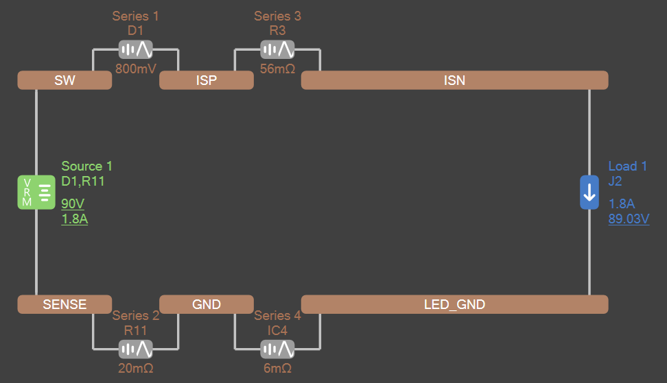
Looking at the current density of the ground and power distribution traces, the maximum is 35A/mm2, which is much lower than we’ve seen in other boards. This should be more than sufficient and also reduce the amount of loss as heat on the planes, keeping the whole board cooler.
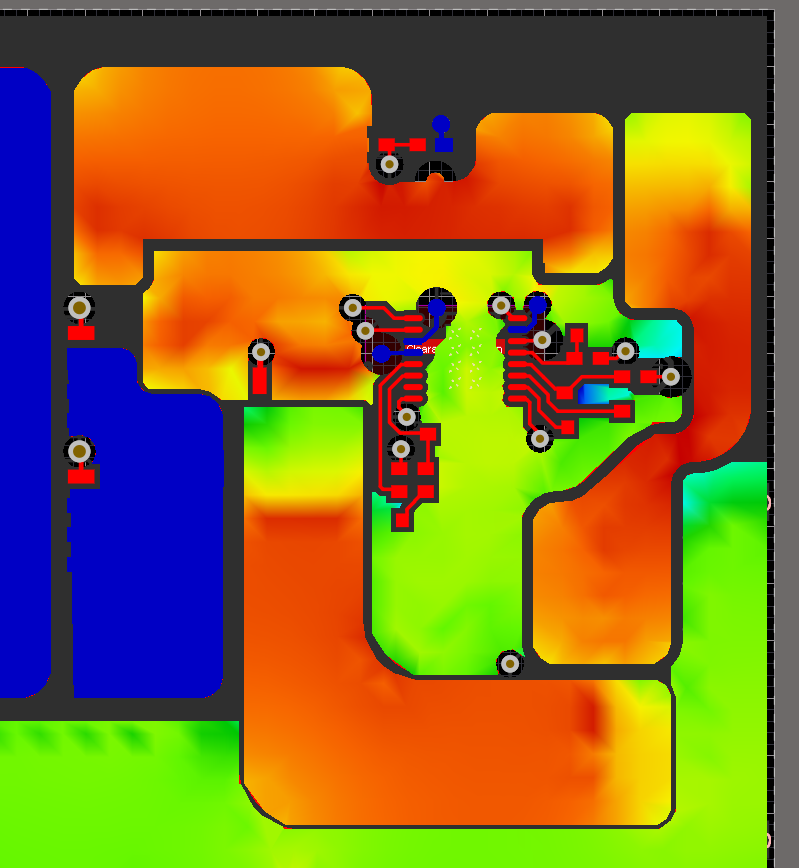
Despite the quick setup of the simulation, knowing that there are no crazy points on this board as far as current density is concerned is good peace of mind.
Final Board Features
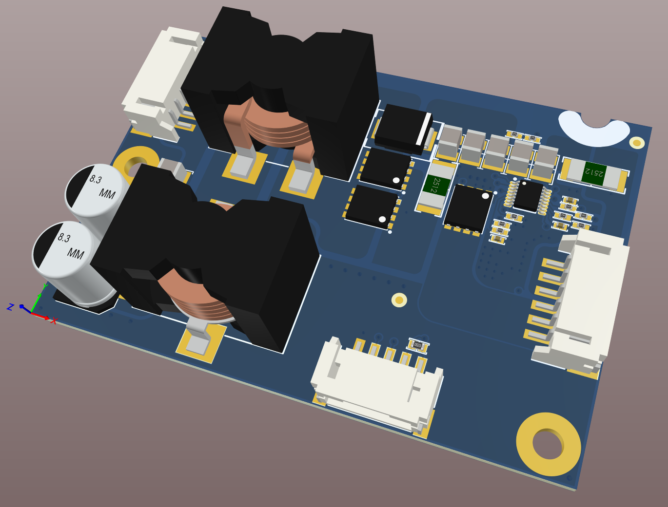
To make this board manufacturable, we need to ensure there are fiducials on the board for the pick and place machine to use. For the board to be usable, it needs a way to be attached to the enclosure. I’ve added M3 mounting holes, as simply using clips from the enclosure is not ideal given the weight of the inductors. With the lack of space along the top of the board for a mounting screw, I have created a cutout in the board outline which will provide enough contact area for a screw to ensure the board cannot move
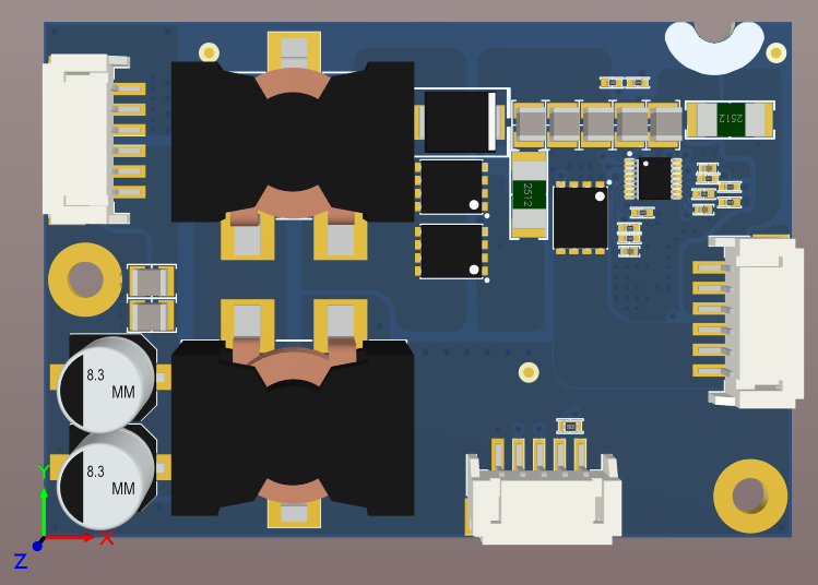
I think the final board looks pretty good. I’m looking forward to designing the LED panel next, and brining all my recent projects together into a complete product.
Finally
As mentioned earlier, you can find the design files for this project on GitHub. It’s free to use as you wish, for any purpose under the MIT license.
This will be a very powerful LED lighting driver, capable of driving over 100 powerful LEDs. Given the voltages on the board, if you decide to build one yourself, you should consider conformal coating to be mandatory. If you are operating the board over 77C, you should consider a heatsink for at least the driver IC, and most likely the MOSFETs and diode as well.