Assembly: The Last Step In The PCB Product Development Process

As pointed out in previous articles, design is the first step in the PCB product development process, so the board designer needs to understand how the downstream processes will impact his design processes/selections/decisions, and this understanding needs to encompass both technical and financial considerations. These deliberations are viewed and weighted as trade-offs. What might make sense from a technical standpoint may not always make sense from a financial one. The goal is to achieve a balance between these two factors and achieve a working, reliable product that is not only cost-effective but will also satisfy projected profit margins.
The last step in this PCB product development process is assembly. The different types of assembly processes—and what needs to be addressed during the design phase to address them—is the subject of this article.
Note: Test is also a downstream effort, but it’s a separate topic and isn’t addressed here, but as with all other factors in the PCB product development effort, the goals are the same: satisfy the technical design requirements and do so in the most economic manner possible.
The Economic Impact of Decisions Made During the Design Process
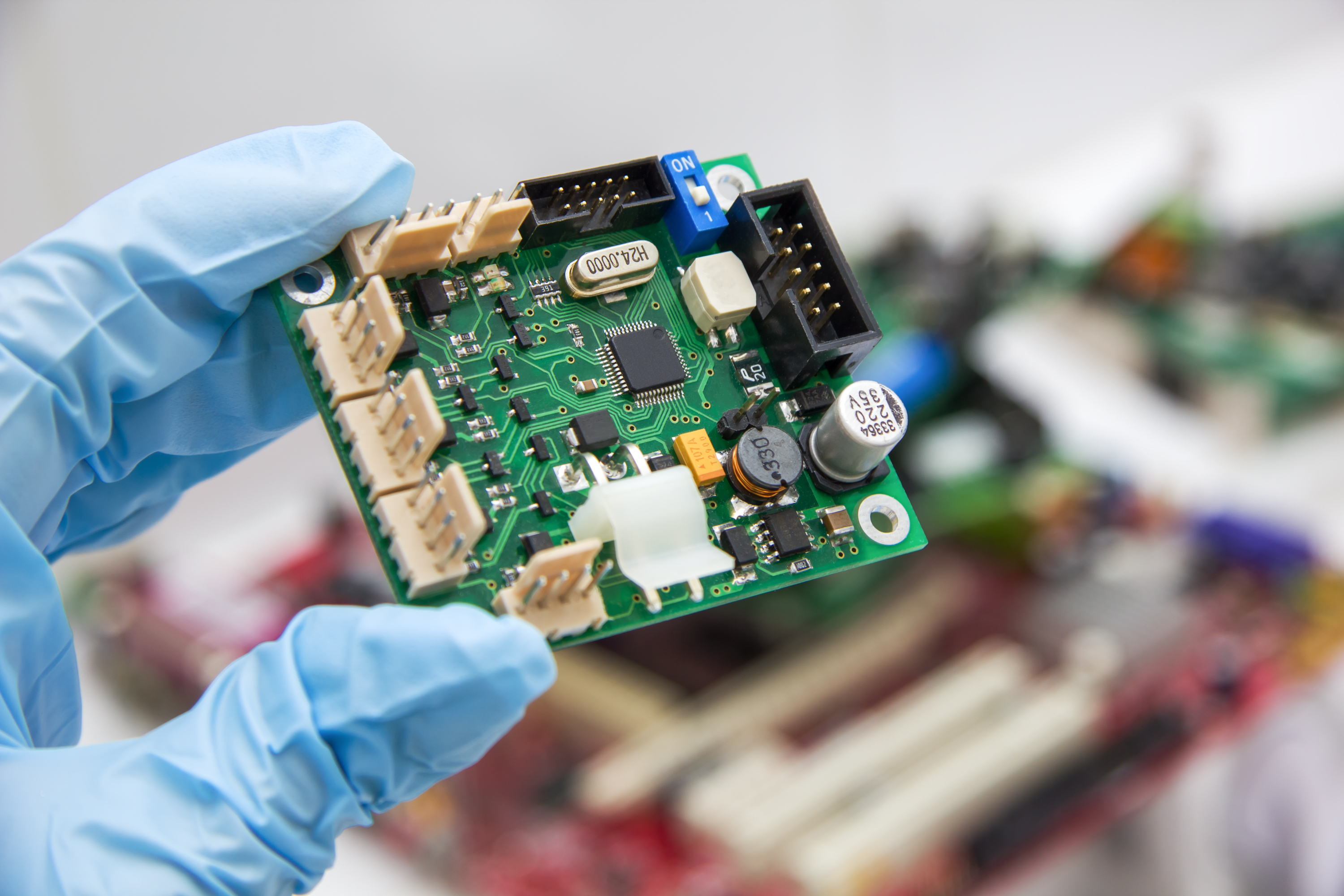
There are four primary types of assembly and subsets of them. They include:
- All through hole
- Through hole with press fit connectors
- Single-sided surface mount
- Double-sided surface mount
- Single-sided surface mount with through hole components
- Double-sided surface mount with through hole components
- The last two types of assembly processes have further variations with press fit connectors.

_15.png)
The above are listed in order of complexity as well as cost. Not surprisingly, as the process becomes more complex it becomes more costly as well. What the different types of assembly processes reflect are the number of trips that have to be made through the assembly line. In terms of the final product’s price and its profit margins, the more trips a board makes through the assembly line, the more expensive it becomes.
The cheapest assembly process is all through hole because the components are typically attached to the board with wave solder.
The Impact of Further Design Decisions
The impact on assembly operations made during the design process begins with the type and number of components selected. This is a decision typically made by the design engineer, and factors to consider during this process include the following:
- It’s best practice not to pick a particular single component that necessitates an additional step in the assembly process.
- This is part of the trade-off between design and cost. It’s best to populate boards with the same types of components that will require the same assembly process. If the particular component is a “make or break” element for the success of the product, the additional cost resulting from this component will need to be factored in all the way from the design effort through final assembly and rework (more about rework below).
- With surface mount components, it’s wise to try to get all the parts on one side of the board. Products that require components on both sides of the board add another level of complexity and cost across all the operations—design, fabrication and assembly.
- In terms of rework, fine pitch QFPs (quad flat packs) will require more rework because of the solder bridges associated with these components.
- A solder bridge forms when two or more pads which are not supposed to be electrically connected on a circuit board are connected. This is due to excessive solder creating a bridge between the pads. In turn, this bridge creates an electrical short that can significantly disrupt the entire operation of a PCB.
- For surface mount assemblies, the components that will result in the least amount of rework steps and cost are BGA packages.
- The choice of a BGA, which at first blush may seem the most expensive option, will end up being a more cost-effective decision than a lower-priced QFP. The BGA will require very little if any rework while a QFP can require a lot of rework which makes the assembly process more complicated as well as more costly. This is one of the biggest mistakes most often made in the PCB product realization effort—picking a component based on price and not on cost.
Lee Ritchey, Founder and President of Speeding Edge notes, “This happened all the time when I was working at 3Com. Product developers would not select a BGA package because ‘it cost more.’”
He continues, “What was surprising, was that it was the people on the assembly side who were making the argument for the use of QFPs based on the BOM (bill of materials) costs. The BOM cost was too much based on the purchase price of the BGAs. Instead of properly weighing the design versus costs trade-offs, they were only looking at the bottom-line costs of the finished product. There was dramatic proof of this in the company’s assembly lines that were in operation in Ireland. At the end of the BGA line there were no PCBs requiring rework while at the end of the QFP line, there were racks and racks of PCBs requiring rework because of solder shorts.”
Further Thoughts on Components
Almost all of the IC components used in today’s products are single-sourced (such as those provided by Intel or other major chip manufacturers). This means, ultimately, they cost what they cost because no other resources exist for them. But, there are other devices beyond ICs that are mounted onto PCBs, and their availability and their viability factors into the overall board design.
Ritchey explains, “The cell phone market pretty much drives the world these days. And, these companies want us to use 0402 capacitors because they are smaller and more readily fit into the cell phone form factor. We have been designing with 0603 capacitors for many years and they are our preference from a design standpoint.”
“The 0402 capacitors are so small and they are very difficult to see. They can end up standing upright on the board because of static electricity. This results in a need for rework.”
He adds, “Now there are 0201 capacitors which are even smaller than the 0402s. The 0201s were designed when the FPGA vendors mandated that the capacitors, along with the inductors, had to be placed under the BGA package. These smaller devices were required because they had to fit between the vias. The problem was that, because of static discharge, they would disappear off the board before the soldering was done. So, it’s important to avoid any excessively small parts as they make the assembly process much more complicated and costly. This is one of those instances where not all good things come in small packages.”
“The challenge right now is that the manufacturers of 0603 capacitors have put out notices that they are no longer producing them.”
In the case of the major FPGA vendors, the carrot for these companies is to not cause their customer problems because they want their components to be designed into the next generation of products. The component vendors rely on as much if not more being selected for their customer’s future products.
Ritchey notes, “The only way that major suppliers will change their products is when a customer behemoth comes along that essentially owns their particular market segment. Then the component vendors will change their products to meet the needs of that customer base because it will radically affect their profitability if they don’t.”
Contract Assembler Capabilities
As with other companies who are part of the PCB manufacturing process, different contract assemblers have different capabilities. To ensure that their product will be successfully assembled at the best price possible, design engineers need to do a thorough investigation of potential contract assemblers. As with fabricators, design engineers being able to visit a contract assembler to see their operations can go a long way toward making sure their product will be successfully assembled at the right price. As part of this research effort, it’s helpful if the assembler can show previous products they’ve assembled that have features similar to the product being designed (i.e., “show me products that look like mine”).
Ritchey points out, “The big problem we have right now is finding assemblers in the U.S. who can assemble prototypes. The number of stateside prototype shops that match what is available offshore keeps dropping because the assemblers don’t get the same level of business that U.S.-based fabricators get. We have basically nursed our on-shore fab shops to keep them going. Now, most of the onshore assembly operations have an offshore partner but being able to get a prototype assembled here in the States is still very crucial.”
Summary
The primary issue of concern for design engineers relative to assembly operations is the different types of assembly that are possible along with their projected costs. Specifically, the number of times that a PCB has to go through the assembly steps and the amount of rework required due to component mounting issues becomes the biggest cost adder to these operations. As part of this process, it’s important to keep in mind that the initial cost of a component may be higher, but its final total cost will be lower because it’s easier to assemble with far fewer defects.
Would you like to find out more about how Altium Designer® can help you with your next PCB design? Talk to an expert at Altium.