Altium Designer Helps You Track Reference Designators on Your PCB
Anytime you place a component in a schematic sheet or PCB layout, the component gets assigned a reference designator. This alphanumeric code is shorthand for a specific component and it helps the design team properly communicate specific components between team members, inside design documents, and within printed circuit design software.
Reference designators are not just random sets of letters and numbers, they follow a specific system that designers use to call out specific components in a PCB. With the right design software, you can place and edit reference designators throughout your design documents, including in the PCB layout, component data, and schematics. Your PCB design software also helps you stay synchronized as you place and modify your PCB reference designators.
ALTIUM DESIGNER®
PCB design software with advanced CAD tools for creating components and placing your reference designators.
Every component you place in your schematics, circuit board layout, bill of materials, and many other design documents will have a corresponding reference designator. The reference designator that appears on the PCB will be assigned to a specific component in your design documentation by your ECAD software, or the user can customize the reference designator to have a specific format that is necessary for the current project.
If you’re using the best PCB layout software with an integrated schematic editor, it’s easy to keep reference designators synchronized between schematic sheets and the PCB layout. As you work through your printed circuit project documents, there is the possibility for your schematics, PCB layout, bill of materials, and final manufacturing outputs to become desynchronized. Altium Designer is the best software you can use to ensure your design will have synchronized reference designators throughout your circuit diagram and schematic diagram sheets, as well as your PCB layout and fabrication documentation.
What Are Reference Designators?
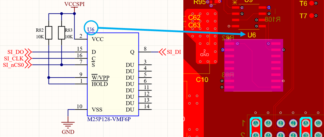
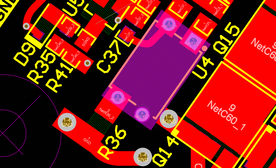
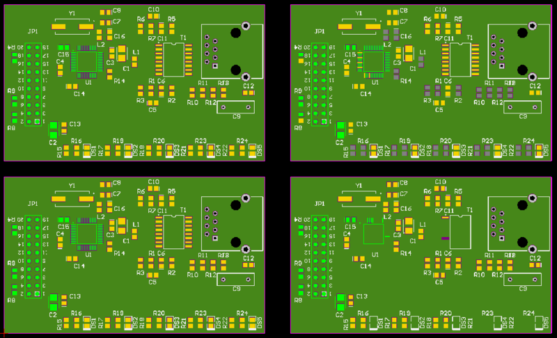
All reference designators appear on the surface layers of a PCB on the silkscreen layers (top and bottom overlay). The reference designator for a component is a letter and number combination assigned to a specific component. Each component gets its own reference designator, meaning reference designators are never repeated. The reference designator for a specific component can be seen in your schematic design documents, PCB layout, and bill of materials as you create the database for your design.

Once Gerber data is generated for your printed circuit layout, the Gerber file with the silkscreen layer data will also include the reference designators for each component. These designators and all other markings in the silkscreen layer will be screen printed onto the solder mask on the PCB as one of the final fabrication steps.
Reference designators are useful for many tasks beyond schematic design and component placement in a PCB layout. The reference designators will also aid any hand assembly tasks, manual inspection, debugging, and testing procedures as specific components in the BOM can be spotted visually in the PCB layout. In addition, reference designators give designers a simple way to see exactly what type of component is on the board without looking at the BOM. This is clear for designers thanks to standardization of reference designators in electrical drawings, and the same standardization is enforced in ECAD software like Altium Designer.
Common PCB Reference Designators
There are two standards that dictate a reference designator format for 45 different types of electronic components that appear in electrical drawings, including schematic sheets and the corresponding printed circuit layout. These are the IEEE 315-1975 and ASME Y14.44-2008 standards. These standards specify the letter prefix that should be used for a given type of component in the PCB layout.
The list below shows a few of the common reference designator prefixes used in circuit board design software:
- U: Integrated circuit
- C: Capacitor
- R: Resistor
- L: Inductor
- J: Connector
- F: Fuse
- Y: Crystal oscillator
- Q: Discrete transistor
Each of these will be numbered in succession to denote specific components in the schematics, bill of materials, and PCB layout. When you create your schematic symbols and PCB footprints for components and you start building up your project libraries, you’ll have an opportunity to define the reference designator prefix for custom or specialty components. You’ll also be able to place the reference designator where you want it around the component.
- Use the CAD tools in Altium Designer to quickly create accurate PCB footprints with standard reference designators.
Learn more about creating a PCB footprint in Altium Designer. - The best ECAD software will enforce consistent reference designators across your design documents and your manufacturing outputs.
Learn more about generating manufacturing outputs with accurate reference designators. - If you need to find standard components in the PCB supply chain, use the Manufacturer Part Search Panel in Altium Designer. This utility gives you access to PCB footprints that contain correct reference designators, pinouts, and land patterns.
Learn more about the Manufacturer Part Search Panel in Altium Designer.

Keep Your PCB Reference Designators Synchronized
The most important aspect of defining reference designators is to ensure they stay synchronized throughout your PCB layout and schematics. In addition, when you generate your bill of materials, the program you use should pull your supplier, part number, and reference designator data directly from your PCB layout and schematics. You shouldn’t have to manually compile this information into a table for your manufacturer. Instead of doing this manually, you need CAD tools that synchronize all of your design documents and fabrication outputs in a single program.
Altium Designer Synchronizes All Design Documentation and Your BOM
The ActiveBOM utility and the integrated schematic editor in Altium Designer are the two critical tools you need to keep your design synchronized. These features are included in Altium Designer alongside the PCB editor, and the integrated design rule engine automatically checks for synchronization errors as you build your board.
In addition to setting reference designators, Altium Designer includes features to help you stay productive by automatically updating changes across design documents. It’s easy to set reference designators and apply updates across your components as you create your design. No other program makes it this easy to ensure your design database stays synchronized.
- Everything from electrical to mechanical parts can be automatically placed in your bill of materials in Altium Designer. The reference designators in your PCB layout will be automatically reflected in your bill of materials.
Learn more about the data in your bill of materials in Altium Designer. - Altium Designer helps you stay productive with a reference designator annotation feature that automatically iterates your reference designators while working in the schematic editor and PCB layout.
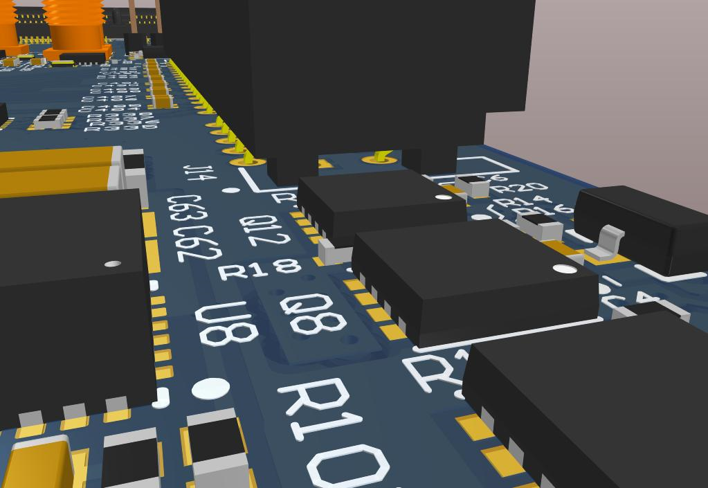
Learn more about reference designator annotation in Altium Designer. - ECAD designers can get a realistic view of the board in 3D to evaluate assembly and reference designator placement in Altium Designer.
Learn more about native 3D design in Altium Designer.

Generate Your Manufacturing Deliverables With Complete Designators
Once you’re ready to prepare your design for fabrication and assembly, you can quickly generate each file needed by your manufacturer inside Altium Designer. The OutJob file feature instantly takes your PCB component data and your layout information, and it generates standard deliverables needed by fabricators and assemblers. The deliverables you create in Altium Designer will include reference designators and sourcing information for your components, helping ensure accurate assembly and aiding debugging and testing tasks after manufacturing.
Stay Productive and Efficient in Altium’s Rules-Driven Design Software
Altium Designer’s complete set of circuit board design tools that work together to help you stay productive and efficient. The documentation features that you’ll use to prepare manufacturing outputs will take data directly from your PCB layout thanks to the application’s powerful rules-driven design engine. This complete set of utilities in Altium Designer create an efficient workflow with an intuitive user interface that isn’t found in other design applications.
- Altium Designer gives you everything needed to create your design data and prepare documentation for your circuit board layout. Altium gives you the best PCB design tools to help you stay at the cutting edge of new technology.
Learn more about Altium Designer’s complete toolset for printed circuit board design. - All Altium Designer users can push their design, fabrication, and assembly data to your manufacturing partners with the Altium 365 platform, the industry’s only managed cloud platform for design collaboration.
Learn more about sharing your PCB project data with Altium 365. - In order to best evaluate placement of components, mechanical designers can import a copy of a team member’s PCB layout into popular mechanical applications using the MCAD CoDesigner extension.
Learn more about the MCAD CoDesigner extension for Altium Designer.

When you need to build the most accurate CAD database for PCB design, ou need the complete set of component creation and management tools in Altium Designer. Get access to the industry’s best ECAD utilities for creating your PCB layout and prepare your manufacturing outputs.
Altium Designer on Altium 365 delivers an unprecedented amount of integration to the electronics industry until now relegated to the world of software development, allowing designers to work from home and reach unprecedented levels of efficiency.
We have only scratched the surface of what is possible to do with Altium Designer on Altium 365. You can check the product page for a more in-depth feature description or one of the On-Demand Webinars.
