
12V DC Uninterruptible Power Supply
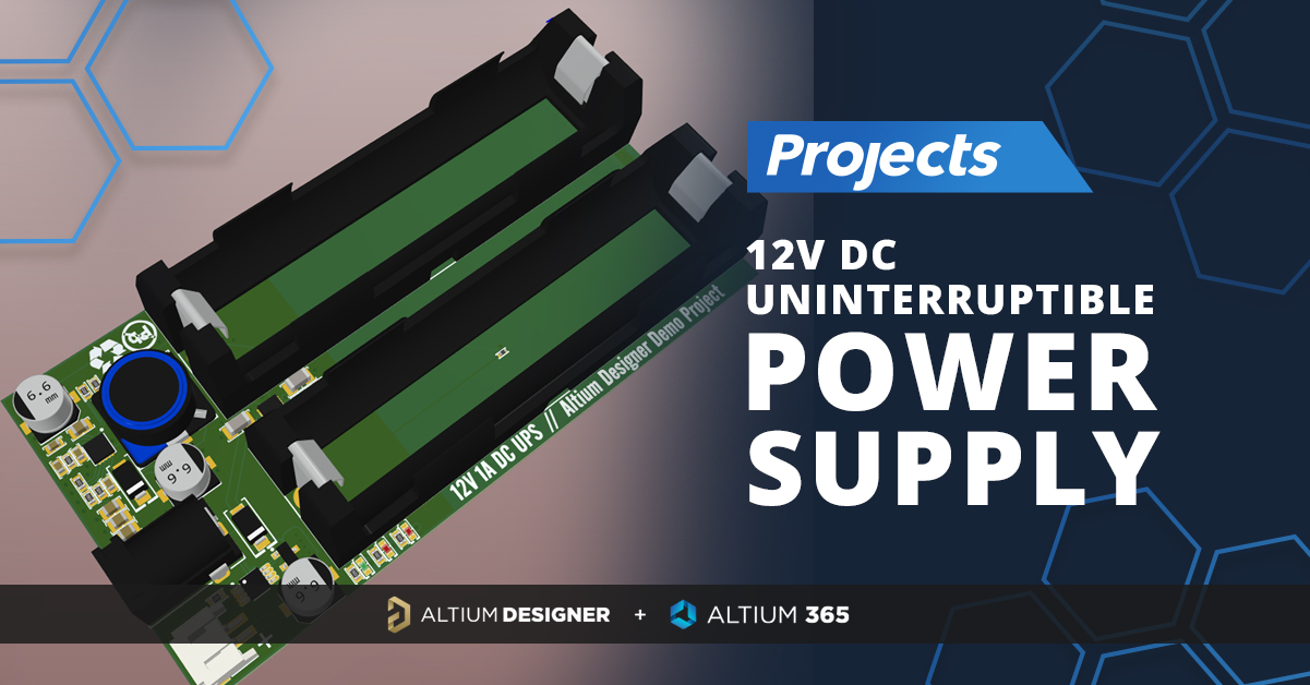
I live in a rural village that tends to have intermittent power when there are high winds or storms. Because of this, my computers, servers, and network equipment are all on relatively low-cost, uninterruptible power supplies. These all run on sealed lead acid batteries and are not an overly efficient way to power a DC device such as a Raspberry Pi or internet router as the incoming mains. AC charges a DC battery, which then creates AC power through an inverter, which powers an AC-DC converter to provide power to the DC device. I thought it would be interesting to make a small UPS suitable for powering my ADSL router, rather than having a whole AC UPS dedicated to it.
My ADSL router has a 12V/1A supply, despite the fact it’s probably running at 1.8-3.3v internally. In this project, I will be creating a 12V 1A UPS. As usual, you can find the open source Altium Designer project files on GitHub, licensed under the MIT license. This license essentially allows you to do what you like with the design. If you’re looking for the library files, this project was designed with my Open Source Altium Designer Library.

Above is the PCB design you'll be reading about in the Altium 365 Viewer; a free way to connect with your co-workers, clients, and friends with the ability to view the design or download with the single click of a button! Upload your design in a matter of seconds and have an interactive way to take an in-depth look without any bulky software or computer power.
Batteries
Lead acid batteries are incredibly cost-effective per watt-hour of energy, but I want to build something a little more modern, compact, and lightweight. I will power my UPS with two 18650 lithium polymer cells, as they offer excellent power density, discharge rate, and relatively high-speed charging. If you’re looking to power your next project with a battery, why not take a look at my article on OctoPart about Choosing a Battery Chemistry for Your Project. An 18650 cell is relatively expensive per watt-hour compared to a lead acid battery, but my UPS won’t have a huge load on it.
An LG MJ1 cell has a capacity of 3500mAh, so two in series provides me with a nominal 25.9Wh. It’s not a lot, but with a 95% efficient DC-DC converter, I will have around 24.6Wh usable offering around two hours of run time at the rated 1A load. In reality, this will likely run my router for five to six hours.
I could use a single cell, or two cells in parallel, however, the two in series allows me to build a more efficient boost converter and offers many more options for monolithic boost converters.
To mount the batteries on the board, I’m taking the easy route and using two Keystone 1043 moulded battery holders. They are cheap enough for me and hold the cells tightly. The cheaper ways of using through hole battery tabs at each end of the cell would require additional effort to hold the cells in place securely—such as a 3d printed enclosure that would do the job the Keystone 1043 battery holder is fully capable of doing.
Battery Charger
For charging the batteries, I will use the Skyworks AAT3663IWO-8.4-2-T1, a two-cell LiPo charger with a 10k NTC thermistor input for thermal protection. The thermistor may not be particularly useful in this design. It won’t quite touch one battery, never mind both—but it is a very useful option when using a pouch cell pack that has a built-in thermistor. I’ll still be adding a thermistor to the board, but it will only be mounted under one cell.
The AAT3663 allows charging the two cells in series at up to 1A, which will give me about a 3 hour recharge time. This is much better than I would get from a lead acid battery, which might be up to 24hrs. The fast recharge time somewhat makes up for the cells’ relatively low capacity in my UPS design, allowing it to handle many short, intermittent power drops on a stormy day due to the short recovery time.
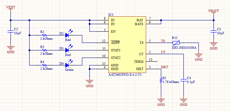
The schematic is very simple to implement, and everything is pretty much just the datasheet recommended values—there isn’t much to think about for this. The ISET resistor R5 sets the current to the maximum 1A. The LEDs are for displaying charge status.
Ideally, a two-cell charger should balance the cells and ensure that one cell doesn’t get overcharged. An overcharged/overvolted cell could be a fire hazard, so it’s something to be aware of. The cells I’m planning to use are quite well matched, so this will just require me to check the cell voltages every other month or so manually, or take them out to balance on one of my ‘fancier’ chargers. I wasn’t able to find a good low-cost option for a balancing two-cell lithium-ion battery charger in the options I Iooked at, so if you have a great part number, leave a comment on the article with your suggestion!
Battery Failover Controller
There are multiple ways to provide failover to a battery; however, I feel the most elegant solution is the Analog Devices LTC4414. When running on battery, this provides the lowest loss configuration by hot swapping the battery in through a P-Channel MOSFET. The LTC4414 is an incredibly versatile IC allowing all sorts of configurations for load sharing and redundant supplies, it’s an IC I’m looking forward to using in other projects in the future.
This isn’t the perfect solution. However, it has a few drawbacks—when running off the AD-DC converter that was included with the router, the schematic has this input running through a diode that provides a voltage drop and losses as heat. The diode I’ve chosen has the lowest forward voltage drop of any SMA diode for it’s current and voltage rating that I was able to find at the suppliers I use. My router continues to operate well below 12V, so this small voltage drop will not be an issue for my application. Other topology options available would use a P-Channel MOSFET for the external supply, which would remove this voltage drop. However, I did not test that topology with a battery charger, so I’m playing it safe by using what I could test.
The other drawback is that the external input (the mains powered supply) must be at least 20mV higher potential than the failover supply for it to use the external supply. If the voltage sags from the wall supply, it will actually start load sharing with the battery backup to stabilize the voltage. This could be a very useful feature in other projects, but it’s probably not going to be of much use for this project. I played with this using my lab power supply, and the IC I was testing was starting to enable the gate as soon as the redundant supply was within 20mV of the external supply.
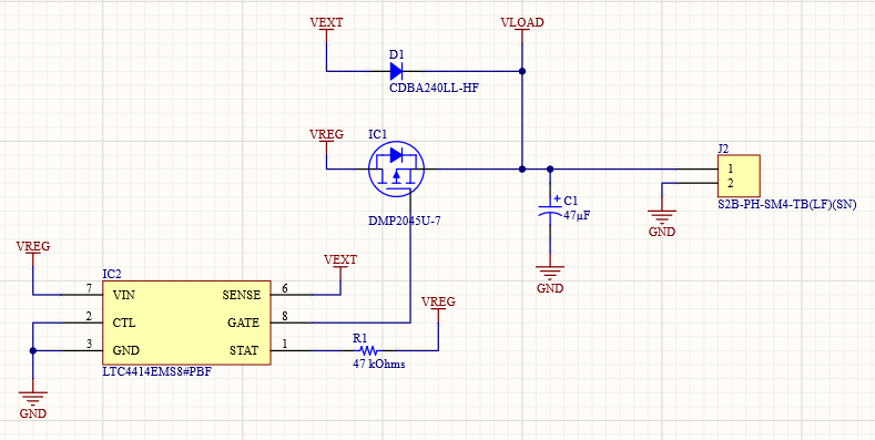
VEXT is the external voltage supply, and VREG is the boosted battery voltage.
I’m using a JST PH connector for the output, as I can easily get a JST PH (or KR, which is compatible) to barrel jack connector for plugging into my router.
Boost Regulator
As I mentioned above, the external input voltage needs to be at least 20mV higher than the redundant supply voltage. Therefore, I’m not going to build a 12V regulator. Instead, I’m going to build an 11.75V regulator. You’re probably thinking, ‘well that’s 250mV lower than the output, surely you can do better than that?’ Well, I thought so too, but after about 10 minutes of playing with resistor values, I decided that 11.75V would be good enough. I’m using the Analog Devices LT8362 for a boost controller, and it has a 1.6V feedback and under-voltage lockout input which is a little nonstandard. The best I could get without tolerances on the resistors getting me too close to 11.98V was 11.75V or using 0.1% or 0.5% resistors with decent resistor values. So I’m building an 11.75V regulator for the redundant supply! This should also allow for voltage sag on the supplied AC-DC regulator and some allowance for the tolerance on the wall supply.
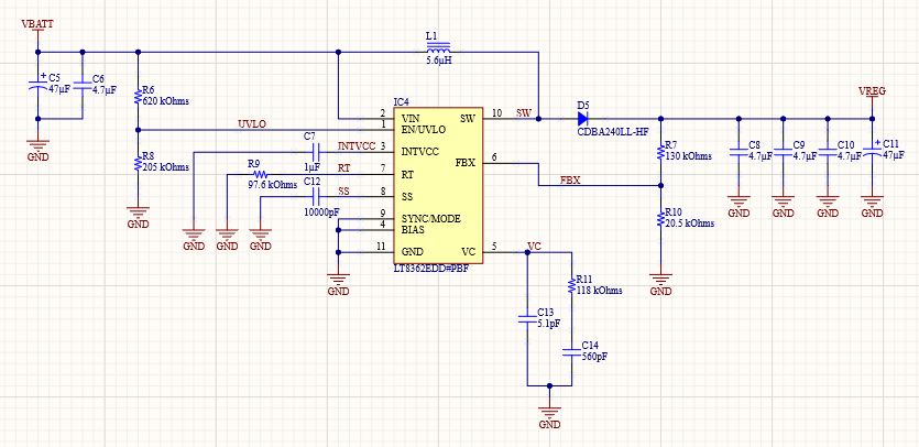
This design simulates to 95% efficient at 500kHz switching frequency. I could gain a very tiny bit more efficiency by dropping down to the minimum 300kHz the device supports; however, the inductor then grows too big for my target board size. Running at a lower frequency only provides a small efficiency gain, so the tradeoff for a slightly smaller size is worth it to me.
I have the under voltage lock outset to 6.4V, so when the cells are at a relatively low, yet still safe discharge state, the regulator will stop providing power. I wouldn’t want either cell to go below 2.9V (5.8V series), and 3.2V is considered a safe point to discharge a lithium-ion cell. The batteries I’m using do not have built-in cell protection, so the regulator switching itself off once the battery voltage reaches the minimum safe point is fairly important.
I haven’t bothered to disable the regulator when the external power supply is present, and the regulator is always on and always ready for a failover scenario. When testing the bench’s design, the switch over from one supply to the other was instantaneous and with no drop in voltage, even with a 200mA load and no output capacitance. Having an always-on regulator will ensure the UPS is ready at a nanosecond’s notice to take over or supplement the external supply if its voltage starts to sag under load. With the battery being trickle charged whenever the external supply is connected, I’m not worried about the inefficiency of keeping the regulator on with no load.
PCB Design
I have a particular spot I want to put this UPS on, so I’m trying to keep the design to 100mm x 50mm. I could easily cheat and put the batteries on the bottom of the board, giving me a lot of real estate on the top for all the components. However, I have to admit I like the look of the batteries and components on one side! I like doing layouts in compact areas, it’s always an interesting challenge to layout and route without making too many sacrifices to the design!
After a bit of playing around, I have the board roughly laid out in a way that mostly makes sense to me. The biggest challenge is the relatively gigantic inductor for the 11.75V regulator. The regulator’s layout is driven by the IC’s pinout and the need to reduce the current loop size as much as possible, so there are only really two ways the regulator can be arranged—as it is, or rotated 180 degrees.
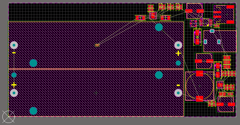
I wasn’t really happy with the location of the charger IC up against the top edge of the board; there isn’t a lot of area for copper heatsinking up there. I also realized that the batteries should be swapped around, so the positive terminal is closest to the switched-mode power supply input. Having the voltage regulator between the two cells improved the layout for the battery charger and the regulator. I originally had the positive terminal towards the top edge of the PCB to optimize the distance to the charger, which I had placed on the board first. However, this increased the distance to the voltage regulator and did not provide a great current path from the positive terminal to the regulator input. The re-arranged board is far better, and I’m happy with it.
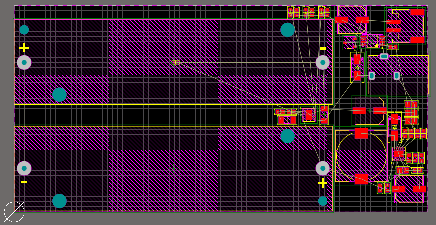
The component out under the battery holder is the NTC thermistor to terminate charging if the battery gets too hot or to charge the battery very slowly if the cell is too cold. As I mentioned earlier in the article, it’s probably not going to be overly effective protection. It can only sense one battery cell, and not have a good contact for even that job. When designing the schematic, I debated whether to include the thermistor or not, but figured it’s probably better to have inefficient protection rather than none at all.
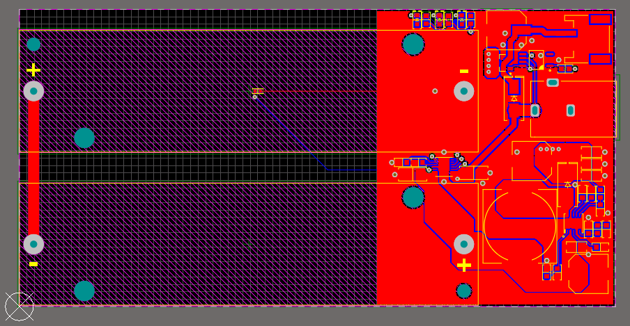
I’m only adding a ground pour around the components, there’s no reason to have copper pour over the rest of the board other than to keep your board manufacturer happy (less chemical usage). Either way, it won’t make much difference electrically to this design.
With the design fully routed, there were not many sacrifices to be made to fit everything in. The board is just long enough to fit the voltage regulator in, with a decent layout and sufficient path for heat to be conducted away.
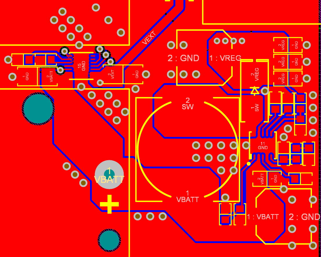
Routing finished, I only shuffled the components and traces around a tiny bit. The final yet important change is to add vias to help move heat from the bottom of the board to the top and ensure a good current path. The battery charger will get warm when it’s at full charge current, as will the voltage regulator. These are both relatively close together, but I’m not bothered by this. There shouldn’t be a time when both of the devices generate heat simultaneously, as either the battery is charging from the external power or the voltage regulator is supplying current to run the connected device. The voltage regulator calculates to about 52c (27c temperature rise) under full load, which is not hot enough to worry about changing the layout or providing a better heat dissipation path.
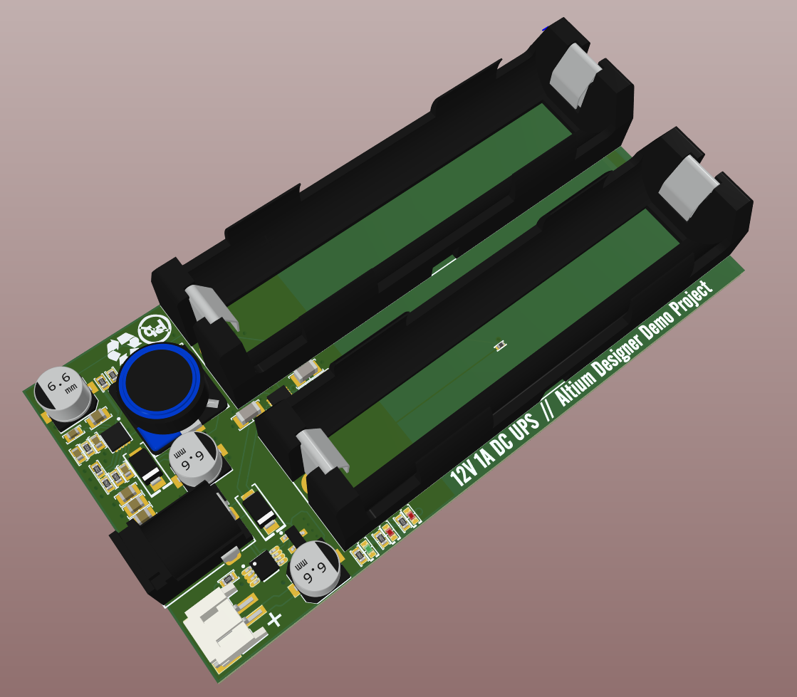
I think the board looks good—the cells with a gap between them for the charger looks better than I had hoped. I’m happy to call this design complete. The charger’s LEDs will be nice and visible along the edge of the board, and the power connectors are easy to use.
Finally
While this is built as a standalone uninterruptible power supply, you can use the concepts within this design to provide a battery backup capability to your own devices. The design files are open source and available on GitHub, as mentioned at the start of the article. With some slight component changes, this design could be adapted to provide a higher output current or different output voltage as your own project requires.
The LTC4414 is a very interesting IC, by far the most versatile OR controller/ideal diode controller IC I’ve looked at in the past years. I’m looking forward to trying it with some other configurations in future projects. The datasheet makes for an interesting read with the wide range of applications presented.
Have more questions? Call an expert at Altium.